3 sleep mode – Rainbow Electronics ATA6630 User Manual
Page 11
11
9117C–AUTO–10/09
ATA6628/ATA6630 [Preliminary]
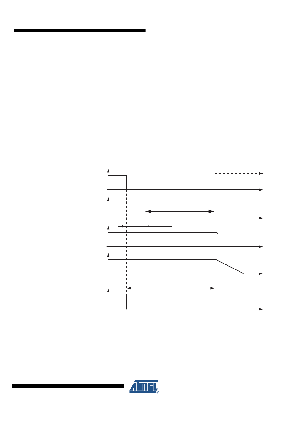
4.3
Sleep Mode
A falling edge at EN when TXD is low switches the IC into Sleep Mode. The TXD Signal has to
be logic low during the Mode Select window (
). In order to avoid any influ-
ence to the LIN-pin during switching into sleep mode it is possible to switch the EN up to 3.2 µs
earlier to Low than the TXD. Therefore, the best an easiest way are two falling edges at TXD
and EN at the same time. The transmission path is disabled in Sleep Mode. The supply current
I
VSsleep
from V
Batt
is typically 10 µA.
The INH output, the PV output and the VCC regulator are switched off. NRES and RXD are low.
The internal slave termination between the LIN pin and VS pin is disabled to minimize the cur-
rent consumption in the event that the LIN pin is short-circuited to GND. Only a weak pull-up
current (typically 10 µA) between the LIN pin and the VS pin is present. Sleep Mode can be acti-
vated independently from the current level on the LIN, WAKE, or KL_15 pin.
A voltage less than the LIN Pre_Wake detection VLINL at the LIN pin activates the internal LIN
receiver and starts the wake-up detection timer.
Figure 4-4.
Switch to Sleep Mode
Del
a
y time
s
leep mode
t
d_
s
leep
= m
a
xim
u
m 20
µs
LIN
s
witche
s
directly to rece
ss
ive mode
t
d
=
3
.2
µs
LIN
VCC
NRE
S
TXD
EN
S
leep Mode
Normal Mode
Mode
s
elect window