Electrical characteristics (continued) – Rainbow Electronics ATA6630 User Manual
Page 27
27
9117C–AUTO–10/09
ATA6628/ATA6630 [Preliminary]
12
NRES Open Drain Output Pin
12.1 Low-level output voltage
V
S
≥
5.5V
I
NRES
= 1 mA
I
NRES
= 250 µA
NRES
V
NRESL
0.2
0.14
V
V
A
12.2 Low-level output low
10 k
Ω
to V
CC
V
CC
= 0V
NRES
V
NRESLL
0.2
V
A
12.3 Undervoltage reset time
V
S
≥
5.5V
C
NRES
= 20 pF
NRES
t
reset
2
4
6
ms
A
12.4
Reset debounce time for
falling edge
V
S
≥
5.5V
C
NRES
= 20 pF
NRES
t
res_f
1.5
10
µs
A
12.5 Switch off leakage current V
NRES
= 5.5V
NRES
–3
+3
µA
A
13
Watchdog Oscillator
13.1
Voltage at WD_OSC in
Normal or Fail-safe Mode
I
WD_OSC
= –200 µA
V
VS
≥
4V
WD_OSC
V
WD_OSC
1.13
1.23
1.33
V
A
13.2 Possible values of resistor Resistor ±1%
WD_OSC
R
OSC
34
120
k
Ω
A
13.3 Oscillator period
R
OSC
= 34 k
Ω
t
OSC
10.65
13.3
15.97
µs
A
13.4 Oscillator period
R
OSC
= 51 k
Ω
t
OSC
15.68
19.6
23.52
µs
A
13.5 Oscillator period
R
OSC
= 91 k
Ω
t
OSC
26.83
33.5
40.24
µs
A
13.6 Oscillator period
R
OSC
= 120 k
Ω
t
OSC
34.2
42.8
51.4
µs
A
14
Watchdog Timing Relative to t
OSC
14.1
Watchdog lead time after
Reset
t
d
7895
cycles
A
14.2 Watchdog closed window
t
1
1053
cycles
A
14.3 Watchdog open window
t
2
1105
cycles
A
14.4
Watchdog reset time
NRES
NRES
t
nres
3.2
4
4.8
ms
A
15
KL_15 Pin
15.1
High-level input voltage
R
V
= 47 k
Ω
Positive edge initializes a
wake-up
KL_15
V
KL_15H
4
V
S
+ 0.3V
V
A
15.2
Low-level input voltage
R
V
= 47 k
Ω
KL_15
V
KL_15L
–1
+2
V
A
15.3 KL_15 pull-down current
V
S
< 27V
V
KL_15
= 27V
KL_15
I
KL_15
50
60
µA
A
15.4 Internal debounce time
Without external capacitor
KL_15
Tdb
KL_15
80
160
250
µs
A
15.5 KL_15 wake-up time
R
V
= 47 k
Ω
, C = 100 nF
KL_15
Tw
KL_15
0.4
2
4.5
ms
C
16
WAKE Pin
16.1 High-level input voltage
WAKE
V
WAKEH
V
S
– 1V
V
S
+ 0.3V
V
A
16.2 Low-level input voltage
Initializes a wake-up signal
WAKE
V
WAKEL
–1
V
S
– 3.3V
V
A
16.3 WAKE pull-up current
V
S
< 27V, V
WAKE
= 0V
WAKE
I
WAKE
–30
–10
µA
A
16.4 High-level leakage current V
S
= 27V, V
WAKE
= 27V
WAKE
I
WAKEL
–5
+5
µA
A
16.5
Time of low pulse for
wake-up via WAKE pin
V
WAKE
= 0V
WAKE
I
WAKEL
30
70
150
µs
A
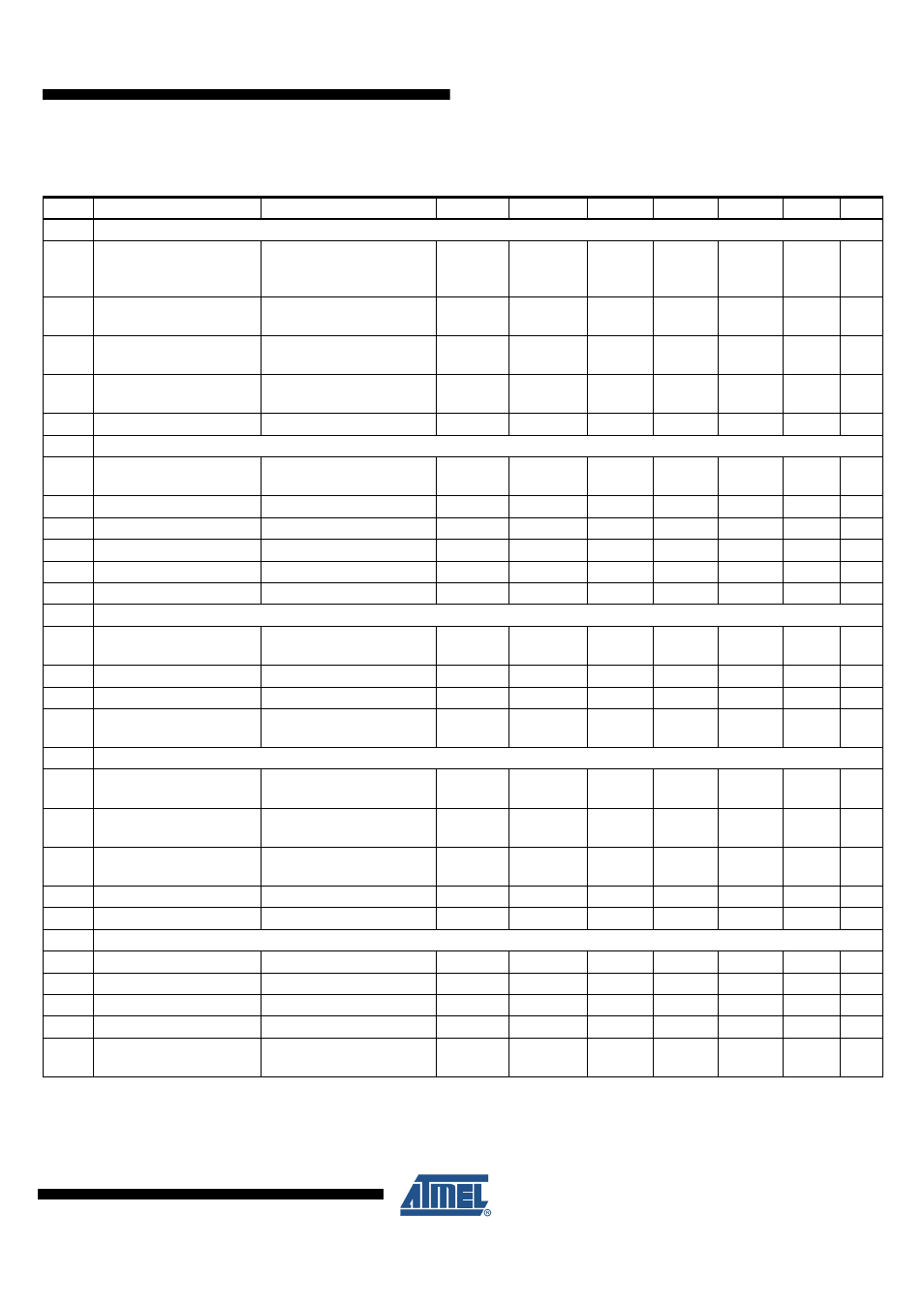
9.
Electrical Characteristics (Continued)
5V < V
S
< 27V, –40°C < T
j
< 150°C, unless otherwise specified. All values refer to GND pins
No.
Parameters
Test Conditions
Pin
Symbol
Min.
Typ.
Max.
Unit
Type*
*) Type means: A = 100% tested, B = 100% correlation tested, C = Characterized on samples, D = Design parameter