5 fail-safe mode – Rainbow Electronics ATA6630 User Manual
Page 15
15
9117C–AUTO–10/09
ATA6628/ATA6630 [Preliminary]
4.5
Fail-safe Mode
The device automatically switches to Fail-safe Mode at system power-up. The voltage regulator
is switched on (V
CC
= 3.3V/5V/2%/50 mA) (see
). The NRES output
switches to low for t
res
= 4 ms and gives a reset to the microcontroller. LIN communication is
switched off. The IC stays in this mode until EN is switched to high. The IC then changes to Nor-
mal Mode. A power down of V
Batt
(V
S
< VS
thU
) during Silent or Sleep Mode switches the IC into
Fail-safe Mode after power up. A low at NRES switches into Fail-safe Mode directly. During
Fail-safe Mode, the TXD pin is an output and signals the fail-safe source. The watchdog is
switched on.
The LIN SBC can operate in different Modes, like Normal, Silent, or Sleep Mode. The functional-
ity of these modes is described in
A wake-up event from either Silent or Sleep Mode will be signalled to the microcontroller using
the two pins RXD and TXD. The coding is shown in
.
A wake-up event will lead the IC to the Fail-safe Mode.
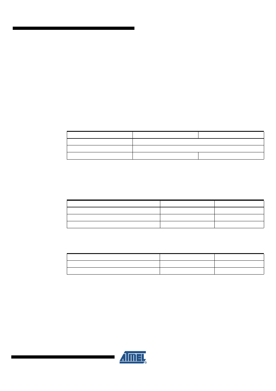
Table 4-2.
TXD, RXD Depending from Operation Modes
Different Modes
TXD
RXD
Fail-safe Mode
Signalling fail-safe sources (see
)
Normal Mode
Follows data transmission
Silent Mode
High
High
Table 4-3.
Signalling Fail-safe Sources
Fail-safe Sources
TXD
RXD
LIN wake-up (pin LIN)
Low
Low
Local wake-up (at pin Wake, pin KL15)
Low
High
VS
th
(battery) undervoltage detection
High
Low
Table 4-4.
Signalling in Fail-safe Mode after Reset (NRES was Low), Shows the Reset
Source at TXD and RXD Pins
Fail-safe Sources
TXD
RXD
VCC undervoltage at NRES
High
Low
Watchdog reset at NRES
High
High