Pin configuration – Rainbow Electronics ATA6624 User Manual
Page 3
3
4986F–AUTO–07/08
ATA6622/ATA6624/ATA6626
2.
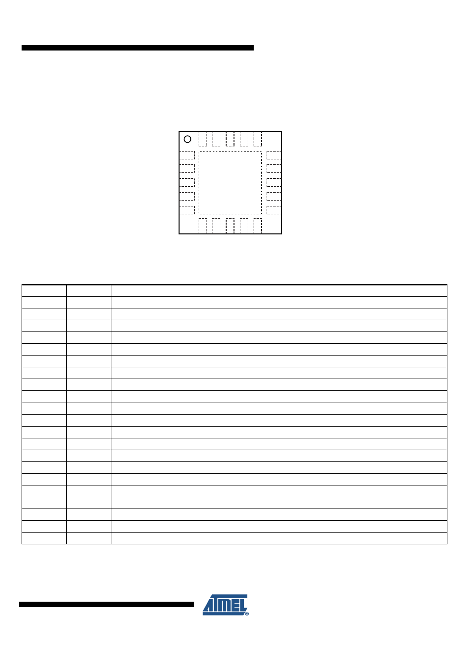
Pin Configuration
Figure 2-1.
Pinning QFN20
6
7
8
10
9
20
19
18
QFN 5 mm
×
5 mm
0.65 mm pitch
20 lead
ATA6622/24/26
16
11
12
13
14
15
TXD
NRES
WD_OSC
TM
MODE
KL15
GND
PVCC
VCC
VS
INH
RXD
GND
LIN
GND
GND
WAKE
NTRIG
GND
EN
5
4
3
2
1
17
Table 2-1.
Pin Description
Pin
Symbol
Function
1
EN
Enables the device in Normal Mode
2
GND
System ground (optional)
3
NTRIG
Low-level watchdog trigger input from microcontroller
4
WAKE
High-voltage input for local wake-up request; if not needed, connect to VS
5
GND
System ground (mandatory)
6
GND
System ground (optional)
7
LIN
LIN-bus line input/output
8
GND
System ground (optional)
9
RXD
Receive data output
10
INH
Battery related output for controlling an external voltage regulator
11
TXD
Transmit data input; active low output (strong pull down) after a local wake-up request
12
NRES
Output undervoltage and watchdog reset (open drain)
13
WD_OSC
External resistor for adjustable watchdog timing
14
TM
For factory testing only (tie to ground)
15
MODE
For debug mode: low, watchdog is on; high, watchdog is off
16
KL_15
Ignition detection (edge sensitive)
17
GND
System ground (optional)
18
PVCC
3.3V/5V regulator sense input pin
19
VCC
3.3V/5V regulator output/driver pin
20
VS
Battery supply
Backside
Heat slug is connected to all GND pins