Electrical characteristics (continued) – Rainbow Electronics ATA6624 User Manual
Page 21
21
4986F–AUTO–07/08
ATA6622/ATA6624/ATA6626
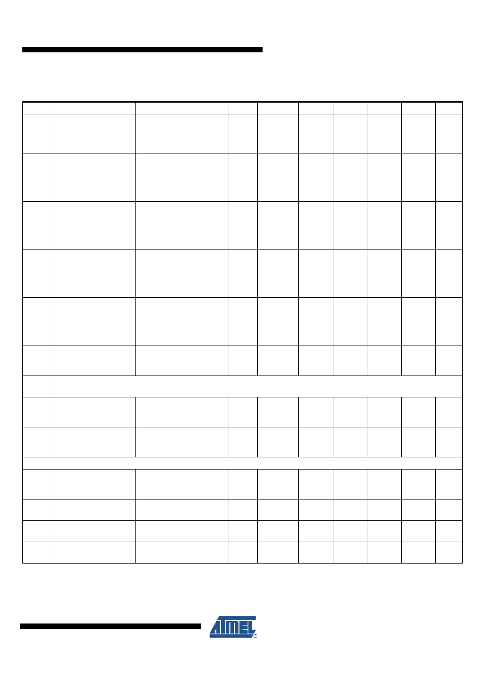
10.5
Time delay for mode
change from Silent
Mode into Normal Mode
via EN
V
EN
= 5V
t
s_n
5
15
40
µs
A
10.6
Duty cycle 1
TH
Rec(max)
= 0.744
×
V
S
TH
Dom(max)
= 0.581
×
V
S
V
S
= 7.0V to 18V
t
Bit
= 50 µs
D1 = t
bus_rec(min)
/(2
×
t
Bit
)
D1
0.396
A
10.7
Duty cycle 2
TH
Rec(min)
= 0.422
×
V
S
TH
Dom(min)
= 0.284
×
V
S
V
S
= 7.6V to 18V
t
Bit
= 50 µs
D2 = t
bus_rec(max)
/(2
×
t
Bit
)
D2
0.581
A
10.8
Duty cycle 3
TH
Rec(max)
= 0.778
×
V
S
TH
Dom(max)
= 0.616
×
V
S
V
S
= 7.0V to 18V
t
Bit
= 96 µs
D3 = t
bus_rec(min)
/(2
×
t
Bit
)
D3
0.417
A
10.9
Duty cycle 4
TH
Rec(min)
= 0.389
×
V
S
TH
Dom(min)
= 0.251
×
V
S
V
S
= 7.6V to 18V
t
Bit
= 96 µs
D4 = t
bus_rec(max)
/(2
×
t
Bit
)
D4
0.590
A
10.10
Slope time falling and
rising edge at LIN
V
S
= 7.0V to 18V Slope
time dominant and
recessive edges
t
SLOPE_fall
t
SLOPE_rise
3.5
22.5
µs
A
11
Receiver Electrical AC Parameters of the LIN Physical Layer
LIN Receiver, RXD Load Conditions: Internal Pull-up R
RXD
= 5 k
Ω
; C
RXD
= 20 pF
11.1
Propagation delay of
receiver (
)
V
S
= 7.0V to 18V
t
rx_pd
= max(t
rx_pdr
, t
rx_pdf
)
t
rx_pd
6
µs
A
11.2
Symmetry of receiver
propagation delay rising
edge minus falling edge
V
S
= 7.0V to 18V
t
rx_sym
= t
rx_pdr
– t
rx_pdf
t
rx_sym
–2
+2
µs
A
12
NRES Open Drain Output Pin
12.1
Low-level output voltage
V
S
≥
5.5V
I
nres
= 1 mA
I
nres
= 250 µA
V
NRESL
0.2
0.14
V
V
A
12.2
Low-level output low
10 k
Ω
to V
CC
V
CC
= 0V
V
NRESLL
0.2
V
A
12.3
Undervoltage reset time
V
VS
≥
5.5V
C
NRES
= 20 pF
T
reset
2
4
6
ms
A
12.4
Reset debounce time for
falling edge
V
VS
≥
5.5V
C
NRES
= 20 pF
T
res_f
1.5
10
µs
A
8.
Electrical Characteristics (Continued)
5V < V
S
< 27V, -40°C < Tj < 150°C, unless otherwise specified. All values refer to GND pins
No.
Parameters
Test Conditions
Pin
Symbol
Min.
Typ.
Max.
Unit
Type*
*) Type means: A = 100% tested, B = 100% correlation tested, C = Characterized on samples, D = Design parameter