Rainbow Electronics AT45DB041B User Manual
Megabit 2.5-volt only or 2.7-volt only dataflash, Features, Description
1
Features
•
Single 2.5V - 3.6V or 2.7V - 3.6V Supply
•
Serial Peripheral Interface (SPI) Compatible
•
20 MHz Max Clock Frequency
•
Page Program Operation
– Single Cycle Reprogram (Erase and Program)
– 2048 Pages (264 Bytes/Page) Main Memory
•
Supports Page and Block Erase Operations
•
Two 264-byte SRAM Data Buffers – Allows Receiving of Data
while Reprogramming of Nonvolatile Memory
•
Continuous Read Capability through Entire Array
•
Low Power Dissipation
– 4 mA Active Read Current Typical
– 2 µA CMOS Standby Current Typical
•
Hardware Data Protection Feature
•
100% Compatible to AT45DB041 and AT45DB041A
•
5.0V-tolerant Inputs: SI, SCK, CS, RESET, and WP Pins
•
Commercial and Industrial Temperature Ranges
Description
The AT45DB041B is a 2.5-volt or 2.7-volt only, serial interface Flash memory ideally
suited for a wide variety of digital voice-, image-, program code- and data-storage
applications. Its 4,325,376 bits of memory are organized as 2048 pages of 264 bytes
each. In addition to the main memory, the AT45DB041B also contains two SRAM data
buffers of 264 bytes each. The buffers allow receiving of data while a page in the main
memor y is being reprogrammed, as well as reading or writing a continuous
data stream. EEPROM emulation (bit or byte alterability) is easily handled with a self-
4-megabit
2.5-volt Only or
2.7-volt Only
DataFlash
®
AT45DB041B
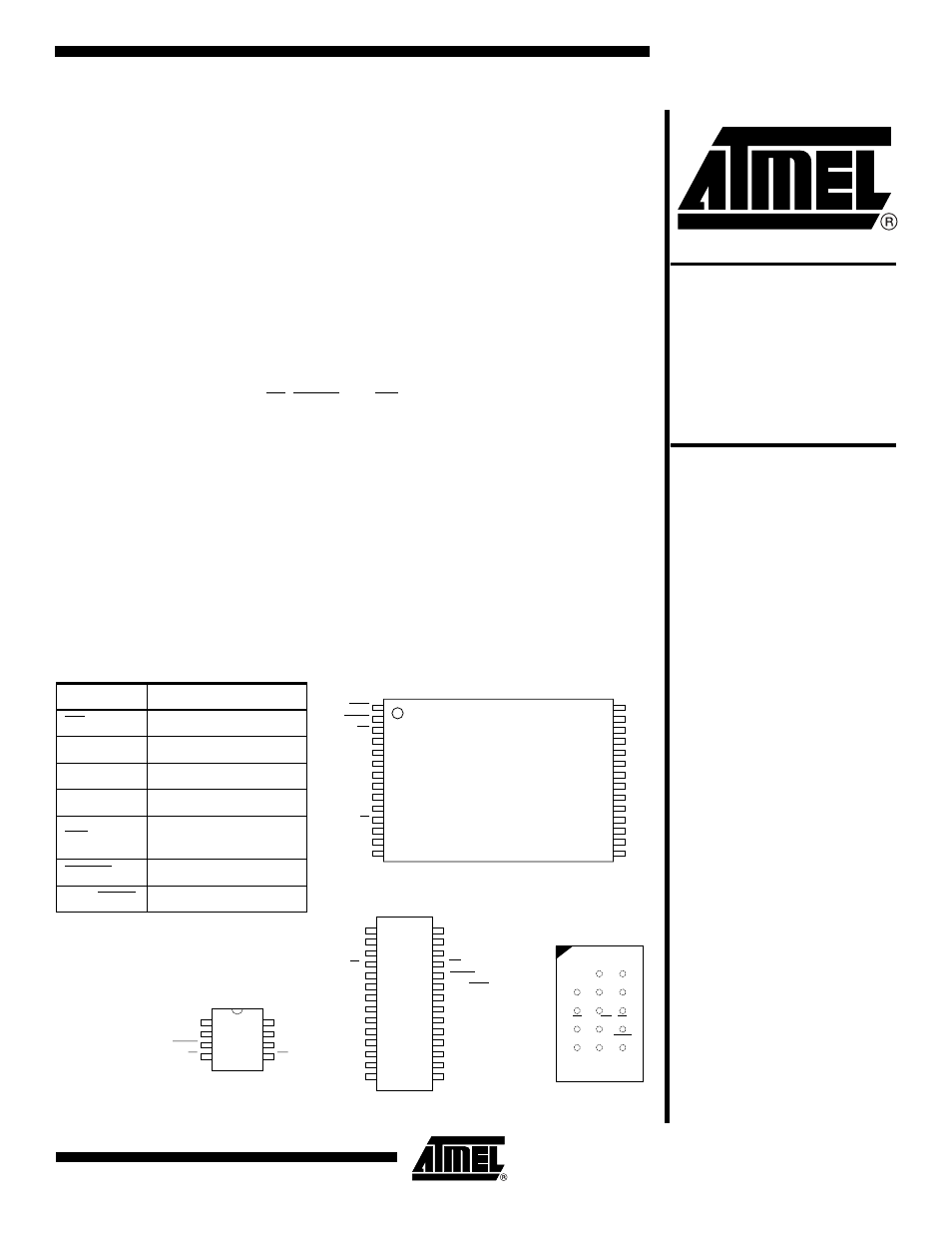
TSOP Top View
Type 1
1
2
3
4
5
6
7
8
9
10
11
12
13
14
28
27
26
25
24
23
22
21
20
19
18
17
16
15
RDY/BUSY
RESET
WP
NC
NC
VCC
GND
NC
NC
NC
CS
SCK
SI
SO
NC
NC
NC
NC
NC
NC
NC
NC
NC
NC
NC
NC
NC
NC
CBGA Top View
through Package
A
B
C
D
E
1
2
3
NC
VCC
WP
RESET
NC
NC
GND
RDY/BSY
SI
NC
SCK
CS
SO
NC
8-SOIC
1
2
3
4
8
7
6
5
SI
SCK
RESET
CS
SO
GND
VCC
WP
28-SOIC
1
2
3
4
5
6
7
8
9
10
11
12
13
14
28
27
26
25
24
23
22
21
20
19
18
17
16
15
GND
NC
NC
CS
SCK
SI
SO
NC
NC
NC
NC
NC
NC
NC
VCC
NC
NC
WP
RESET
RDY/BUSY
NC
NC
NC
NC
NC
NC
NC
NC
Pin Configurations
Pin Name
Function
CS
Chip Select
SCK
Serial Clock
SI
Serial Input
SO
Serial Output
WP
Hardware Page Write
Protect Pin
RESET
Chip Reset
RDY/BUSY
Ready/Busy
Rev. 1938F–DFLSH–10/02
Document Outline
- Pin Configurations
- Features
- Description
- Block Diagram
- Memory Array
- Memory Architecture Diagram
- Device Operation
- Status Register Format
- Block Erase Addressing
- Power-on/Reset State
- Absolute Maximum Ratings*
- DC and AC Operating Range
- DC Characteristics
- AC Characteristics
- Input Test Waveforms and Measurement Levels
- Output Test Load
- AC Waveforms
- Write Operations
- Read Operations
- Detailed Bit-level Read Timing – Inactive Clock Polarity Low
- Detailed Bit-level Read Timing – Inactive Clock Polarity Low (Continued)
- Detailed Bit-level Read Timing – Inactive Clock Polarity High
- Detailed Bit-level Read Timing – Inactive Clock Polarity High (Continued)
- Detailed Bit-level Read Timing – SPI Mode 0
- Detailed Bit-level Read Timing – SPI Mode 0 (Continued)
- Detailed Bit-level Read Timing – SPI Mode 3
- Detailed Bit-level Read Timing – SPI Mode 3 (Continued)
- Sector Addressing
- Ordering Information
- Packaging Information