Read/write time slots, Read/write timing diagram figure 11, Write-one time slot – Rainbow Electronics DS2432 User Manual
Page 26: Write-zero time slot
PRELIMINARY
DS2432
26 of 30
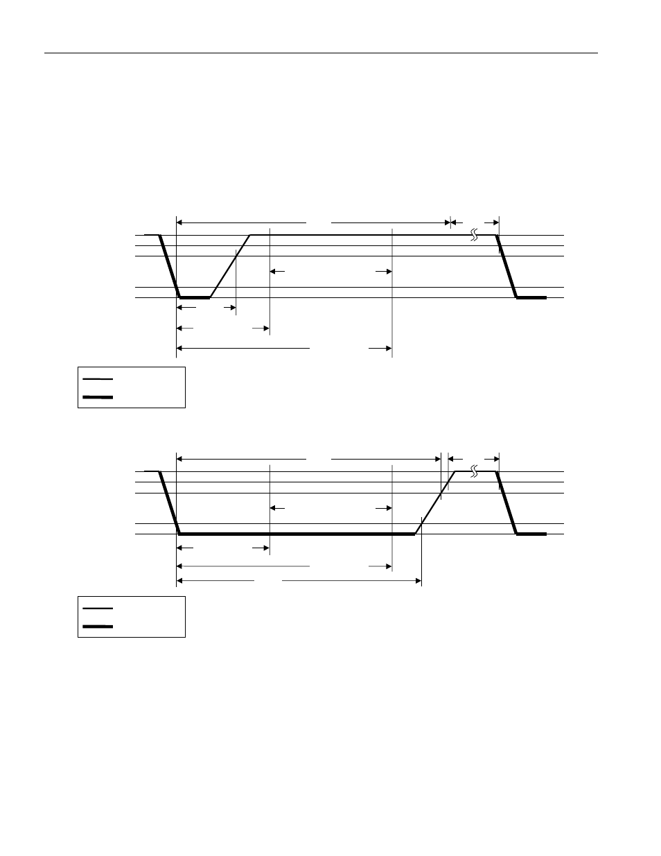
Read/Write Time Slots
The definitions of write and read time slots are illustrated in Figure 11. The master initiates all time slots
by driving the data line low. The falling edge of the data line synchronizes the DS2432 to the master by
triggering an internal delay circuit. During write time slots, the delay circuit determines when the DS2432
will sample the data line. For a read data time slot, if a “0” is to be transmitted, the delay circuit
determines how long the DS2432 will hold the data line low. If the data bit is a “1”, the DS2432 will not
hold the data line low at all.
READ/WRITE TIMING DIAGRAM Figure 11
Write-one Time Slot
V
PULLUP
V
PULLUP MIN
V
IH MIN
V
IL MAX
0V
t
LOW1
15 µs
(OD: 2 µs)
60 µs
(OD: 6 µs)
DS2432
Sampling Window
t
REC
t
SLOT
REGULAR SPEED
60 µs
≤
t
SLOT
< 120 µs
1 µs
≤
t
LOW1
< 15 µs
1 µs
≤
t
REC
<
∞
OVERDRIVE SPEED
6 µs
≤
t
SLOT
< 16 µs
1 µs
≤
t
LOW1
< 2 µs
1 µs
≤
t
REC
<
∞
RESISTOR
MASTER
Write-zero Time Slot
V
PULLUP
V
PULLUP MIN
V
IH MIN
V
IL MAX
0V
REGULAR SPEED
60 µs
≤
t
LOW0
< t
SLOT
< 120 µs
1 µs
≤
t
REC
<
∞
OVERDRIVE SPEED
6 µs
≤
t
LOW0
< t
SLOT
< 16 µs
1 µs
≤
t
REC
<
∞
RESISTOR
MASTER
t
LOW0
15 µs
(OD: 2 µs)
60 µs
(OD: 6 µs)
DS2432
Sampling Window
t
REC
t
SLOT