Rainbow Electronics AT29C020 User Manual
Features, Description, Pin configurations
1
Features
•
Fast Read Access Time – 70 ns
•
5-volt Only Reprogramming
•
Sector Program Operation
– Single Cycle Reprogram (Erase and Program)
– 1024 Sectors (256 Bytes/Sector)
– Internal Address and Data Latches for 256 Bytes
•
Internal Program Control and Timer
•
Hardware and Software Data Protection
•
Two 8K Bytes Boot Blocks with Lockout
•
Fast Sector Program Cycle Time – 10 ms
•
DATA Polling for End of Program Detection
•
Low Power Dissipation
– 40 mA Active Current
– 100 µA CMOS Standby Current
•
Typical Endurance > 10,000 Cycles
•
Single 5V
±10% Supply
•
CMOS and TTL Compatible Inputs and Outputs
•
Commercial and Industrial Temperature Ranges
Description
The AT29C020 is a 5-volt-only in-system Flash programmable and erasable read-only
memory (PEROM). Its 2 megabits of memory is organized as 262,144 bytes. Manu-
factured with Atmel’s advanced nonvolatile CMOS technology, the device offers
access times to 70 ns with power dissipation of just 220 mW over the commercial tem-
perature range. When the device is deselected, the CMOS standby current is less
than 100
µA. Device endurance is such that any sector can typically be written to in
excess of 10,000 times.
2-megabit
(256K x 8)
5-volt Only
Flash Memory
AT29C020
Rev. 0291N–FLASH–07/02
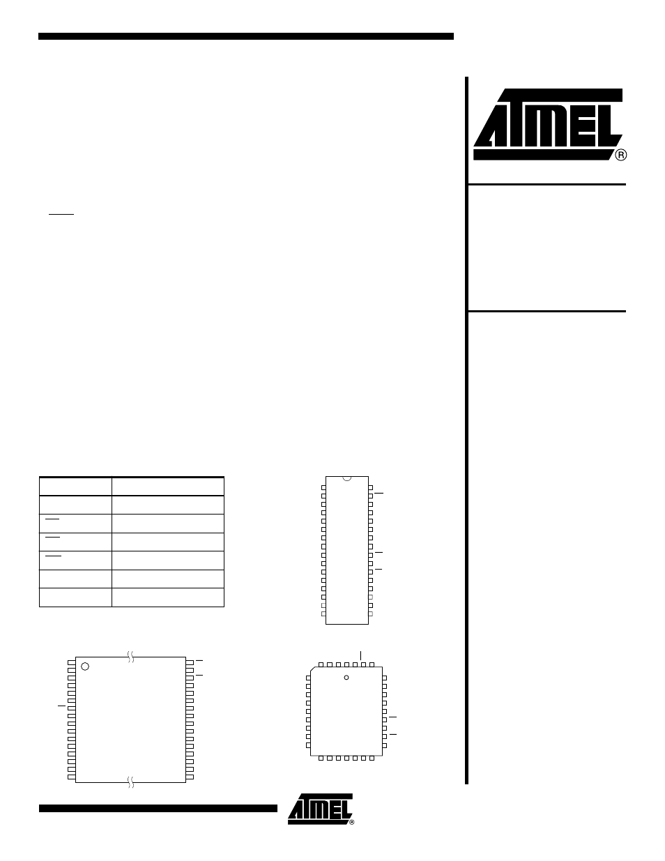
Pin Configurations
Pin Name
Function
A0 - A17
Addresses
CE
Chip Enable
OE
Output Enable
WE
Write Enable
I/O0 - I/O7
Data Inputs/Outputs
NC
No Connect
DIP Top View
PLCC Top View
1
2
3
4
5
6
7
8
9
10
11
12
13
14
15
16
32
31
30
29
28
27
26
25
24
23
22
21
20
19
18
17
NC
A16
A15
A12
A7
A6
A5
A4
A3
A2
A1
A0
I/O0
I/O1
I/O2
GND
VCC
WE
A17
A14
A13
A8
A9
A11
OE
A10
CE
I/O7
I/O6
I/O5
I/O4
I/O3
5
6
7
8
9
10
11
12
13
29
28
27
26
25
24
23
22
21
A7
A6
A5
A4
A3
A2
A1
A0
I/O0
A14
A13
A8
A9
A11
OE
A10
CE
I/O7
4
3
2
1
32
31
30
14
15
16
17
18
19
20
I/O1
I/O2
GND
I/O3
I/O4
I/O5
I/O6
A12
A15
A16
NC
VCC
WE
A17
TSOP Top View
Type 1
1
2
3
4
5
6
7
8
9
10
11
12
13
14
15
16
32
31
30
29
28
27
26
25
24
23
22
21
20
19
18
17
A11
A9
A8
A13
A14
A17
WE
VCC
NC
A16
A15
A12
A7
A6
A5
A4
OE
A10
CE
I/O7
I/O6
I/O5
I/O4
I/O3
GND
I/O2
I/O1
I/O0
A0
A1
A2
A3
Document Outline
- Features
- Description
- Block Diagram
- Device Operation
- Absolute Maximum Ratings*
- DC and AC Operating Range
- Operating Modes
- DC Characteristics
- AC Read Characteristics
- AC Read Waveforms(1)(2)(3)(4)
- Input Test Waveforms and Measurement Level
- Output Test Load
- Pin Capacitance
- AC Byte Load Characteristics
- AC Byte Load Waveforms
- Program Cycle Characteristics
- Program Cycle Waveforms(1)(2)(3)
- Software Protected Program Cycle Waveform(1)(4)(5)
- Data Polling Characteristics(1)
- Data Polling Waveforms
- Toggle Bit Characteristics(1)
- Toggle Bit Waveforms(1)(2)(3)
- Boot Block Lockout FeatureEnableAlgorithm(1)
- Ordering Information
- Packaging Information