Device addressing, Write operations – Rainbow Electronics AT24C1024B User Manual
Page 8
8
AT24C1024B [Preliminary]
5194D–SEEPR–5/07
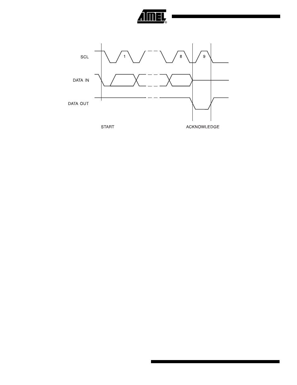
Figure 6. Output Acknowledge
Device
Addressing
The 1024K EEPROM requires an 8-bit device address word following a start condition to
enable the chip for a read or write operation (see Figure 7 on page 11). The device address
word consists of a mandatory one, zero sequence for the first four most significant bits as
shown. This is common to all two-wire EEPROM devices.
The 1024K uses the two device address bit, A1, A2, to allow up to four devices on the same
bus. These A1, A2 bits must compare to the corresponding hardwired input pins. The A1, A2
pin uses an internal proprietary circuit that biases it to a logic low condition if the pin is allowed
to float.
The seventh bit (P
0
) of the device address is a memory page address bit. This memory page
address bit is the most significant bit of the data word address that follows. The eighth bit of
the device address is the read/write operation select bit. A read operation is initiated if this bit
is high and a write operation is initiated if this bit is low.
Upon a compare of the device address, the EEPROM will output a zero. If a compare is not
made, the device will return to a standby state.
DATA SECURITY: The AT24C1024B has a hardware data protection scheme that allows the
user to write-protect the entire memory when the WP pin is at V
CC
.
Write
Operations
BYTE WRITE: To select a data word in the 1024K memory requires a 17-bit word address.
The word address field consists of the P
0
bit of the device address, then the most significant
word address followed by the least significant word address (see Figure 8 on page 11)
A write operation requires the P
0
bit and two 8-bit data word addresses following the device
address word and acknowledgment. Upon receipt of this address, the EEPROM will again
respond with a zero and then clock in the first 8-bit data word. Following receipt of the 8-bit
data word, the EEPROM will output a zero. The addressing device, such as a microcontroller,
then must terminate the write sequence with a stop condition. At this time the EEPROM enters
an internally timed write cycle, T
WR
, to the nonvolatile memory. All inputs are disabled during
this write cycle and the EEPROM will not respond until the write is complete (see Figure 8 on
page 11).