Rainbow Electronics DS1220Y User Manual
Page 7
DS1220Y
091295 7/8
7. If the CE high transition occurs prior to or simultaneously with the WE high transition, the output buffers re-
main in a high impedance state during this period.
8. If WE is low or the WE low transition occurs prior to or simultaneously with the CE low transition, the output
buffers remain in a high impedance state during this period.
9. Each DS1220Y is marked with a 4-digit date code AABB. AA designates the year of manufacture. BB desig-
nates the week of manufacture. The expected t
DR
is defined as starting at the date of manufacture.
10. In a power down condition the voltage on any pin may not exceed the voltage of V
CC
.
11. t
WR1
, t
DH1
are measured from WE going high.
12. t
WR2
, t
DH2
are measured from CE going high.
13. DS1220Y modules are recongnized by Underwriters Laboratory (U.L.
) under file E99151 (R).
DC TEST CONDITIONS
Outputs open.
All voltages are referenced to ground.
AC TEST CONDITIONS
Output Load: 100pF + 1TTL Gate
Input Pulse Levels: 0-3.0V
Timing Measurement Reference Levels
Input:1.5V
Output: 1.5V
Input Pulse Rise and Fall Times: 5ns
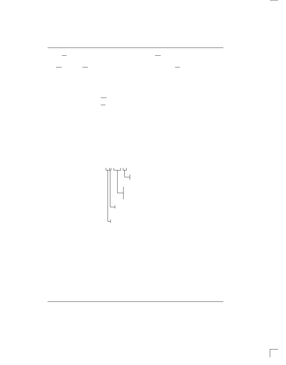
ORDERING INFORMATION
DS1220 TTP– SSS – III
Operating Temperature Range
Blank: 0
°
to 70
°
IND: –40
°
to +85
°
C
Access
100:
120:
150:
200:
Speed
100 ns
120 ns
150 ns
200 ns
Package Type
Blank: 24–pin 600 mil DIP
V
CC
Tolerance
Y: 10%