Typical operating characteristics (continued), Pin description – Rainbow Electronics DS2778 User Manual
Page 7
DS2775/DS2776/DS2777/DS2778
2-Cell, Stand-Alone, Li+ Fuel-Gauge IC with
Protector and Optional SHA-1 Authentication
_______________________________________________________________________________________
7
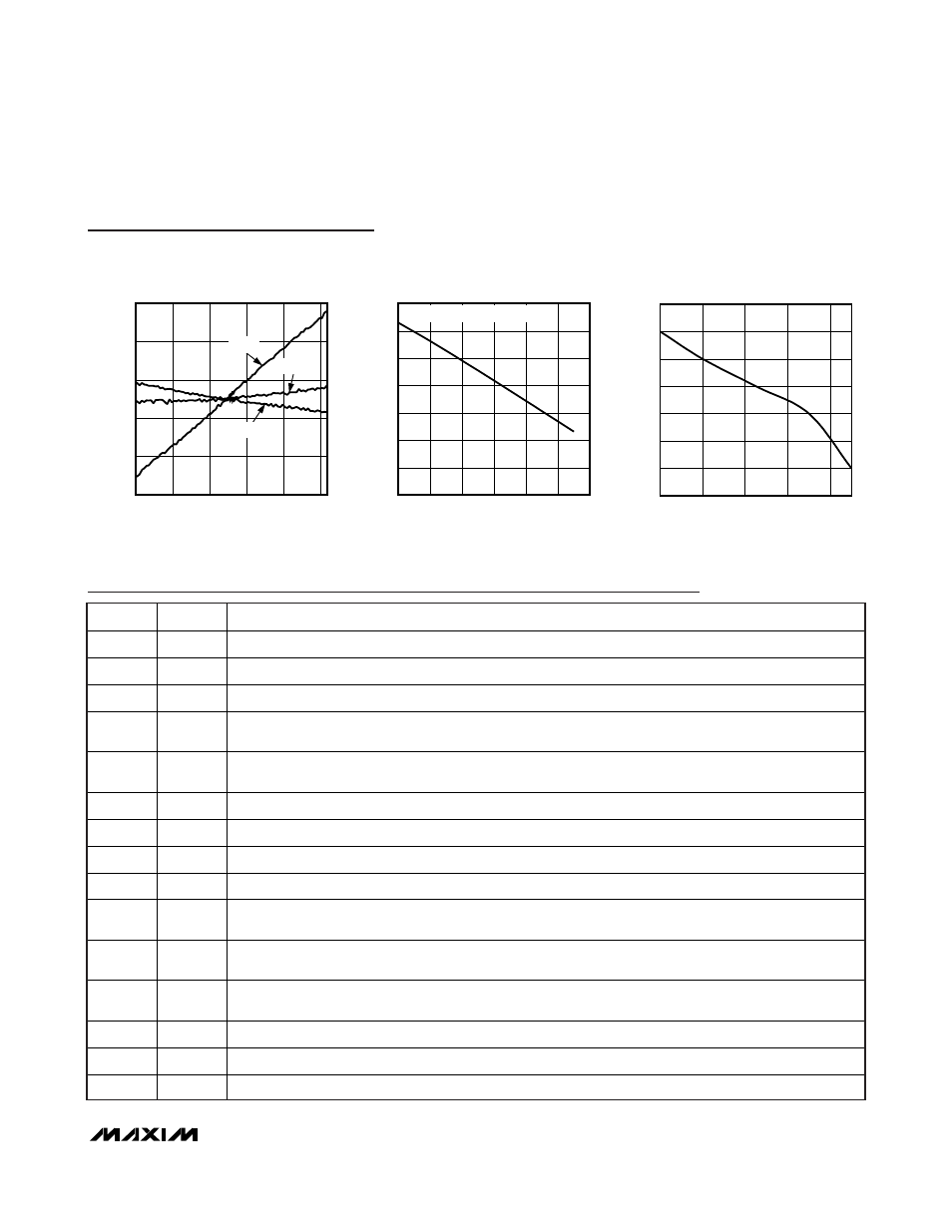
CURRENT MEASUREMENT
ACCURACY
DS2775/6/7/8 toc07
V
SNS
(mV)
ACCURACY (
μ
V)
0.048
0.028
0.008
-0.012
-0.032
-75
-25
25
75
125
-125
-0.052
+70
°C
-20
°C
+25
°C
I
RC
vs. V
DD
DS2775/6/7/8 toc08
V
DD
(V)
I
RC
(mA)
5
4
3
2
1
1
2
3
4
5
6
7
0
0
6
1k
Ω RESISTOR FROM PLS TO PK+
CURRENT MEASUREMENT OFFSET
vs. TEMPERATURE
DS2775/6/7/8 toc09
TEMPERATURE (
°C)
LSB (1.5625
μ
V)
60
40
20
0
-4
-3
-2
-1
0
1
2
-5
-20
Typical Operating Characteristics (continued)
(T
A
= +25°C, unless otherwise noted.)
Pin Description
PIN
NAME
FUNCTION
1
CC
Charge Control. Charge FET control output.
2 V
DD
Chip-Supply Input. Bypass with 0.1μF to V
SS
.
3
DC
Discharge Control. Discharge FET control output.
4 V
IN2
Battery Voltage Sense Input 2. Connect to highest voltage potential positive cell terminal through
decoupling network.
5 V
IN1
Battery Voltage Sense Input 1. Connect to lowest voltage potential positive cell terminal through
decoupling network.
6
VB
Regulated Operating Voltage. Bypass with 0.1μF to V
SS
.
7 V
SS
Device Ground. Chip ground and battery-side sense resistor input.
8
SNS
Sense Resistor Connection. Pack-side sense resistor sense input.
9
PIO
Programmable I/O. Can be configured as wake input.
10 PLS
Pack Plus Terminal Sense Input. Used to detect the removal of short-circuit, discharge overcurrent, and
charge overcurrent conditions.
11 SDA/DQ
Data Input/Output. Serial data I/O, includes weak pulldown to detect system disconnect and can be
configured as wake input for 1-Wire devices.
12 SCL/OVD
Serial Clock Input/Overdrive Select. Communication clock for 2-wire devices/overdrive select pin for
1-Wire devices.
13
SRC
Protection MOSFET Source Connection. Used as a reference for the charge pump.
14
CP
Charge Pump Output. Generates gate drive voltage for protection FETs. Bypass with 0.47μF to SRC.
—
EP
Exposed Pad. Connect to ground or no connection.