Protection, status, and control registers – Rainbow Electronics DS2778 User Manual
Page 24
Protection, Status, and Control Registers
Protection Register Format
The Protection register reports events detected by the Li+ safety circuit on bits [7:2]. Bits 0 and 1 are used to disable
the charge and discharge FET gate drivers. Bits [7:2] are set by internal hardware only. Bits 2 and 3 are cleared by
hardware only. Bits [7:4] are cleared by writing the register with a 0 in the bit position of interest. Writing a 1 to bits
[7:4] has no effect on the register. Bits 0 and 1 are set on power-up and a transition from sleep to active modes.
While in active mode, these bits can be cleared to disable the FET gate drive of either or both FETs. Setting these
bits only turns on the FETs if there are no protection faults.
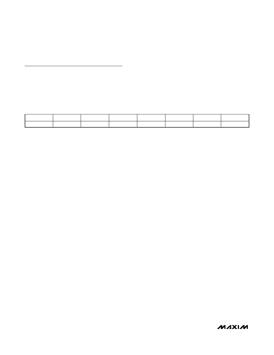
Protection Register (00h)
Bit 7: Overvoltage Flag (OV). OV is set to indicate that an overvoltage condition has been detected. The average of
the voltages on V
IN1
and V
IN2
has persisted above the OV threshold for t
OVD
. OV remains set until written to 0,
cleared by a power-on reset, or transitioned to sleep mode.
Bit 6: Undervoltage Flage (UV). UV is a read-only mirror of the UVF flag located in the Status register. UVF is set to
indicate that the average of the voltages on V
IN1
and V
IN2
has persisted below the UV threshold for t
UVD
. The UVF
bit must be written to 0 to clear UV and UVF.
Bit 5: Charge Overcurrent Flag (COC). COC is set to indicate that an overcurrent condition has occurred while
charging. The sense-resistor voltage has persisted above the COC threshold for t
OCD
. COC remains set until written
to 0, cleared by a power-on reset, or transitioned to sleep mode.
Bit 4: Discharge Overcurrent Flag (DOC). DOC is set to indicate that an overcurrent condition has occurred while
discharging. The sense-resistor voltage has persisted above the DOC threshold for t
OCD
. DOC remains set until writ-
ten to 0, cleared by a power-on reset, or transitioned to sleep mode.
Bit 3: Charge Control Flag (CC). CC indicates the logic state of the CC pin driver. The CC flag is set to indicate CC
high and is cleared to indicate CC low. The CC flag is read-only.
Bit 2: Discharge Control Flag (DC). DC indicates the logic state of the DC pin driver. DC flag is set to indicate DC
high and is cleared to indicate DC low. DC flag is read-only.
Bit 1: Charge-Enable Bit (CE). CE must be set to allow the CC pin to drive the charge FET to the on state. CE acts
as an enable input to the safety circuit. If all safety conditions are met and CE is set, the CC pin drives to V
CP
. If CE
is cleared, the CC pin is driven low to disable the charge FET. The power-up default state of CE is 1.
Bit 0: Discharge-Enable Bit (DE). DE must be set to allow the DC pin to drive the discharge FET to the on state. DE
acts as an enable input to the safety circuit. If all safety conditions are met and DE is set, the DC pin drives to V
CP
. If
DE is cleared, the DC pin is driven low to disable the discharge FET. The power-up default state of DE is 1.
DS2775/DS2776/DS2777/DS2778
2-Cell, Stand-Alone, Li+ Fuel-Gauge IC with
Protector and Optional SHA-1 Authentication
24
______________________________________________________________________________________
BIT 7
BIT 6
BIT 5
BIT 4
BIT 3
BIT 2
BIT 1
BIT 0
OV UV COC
DOC
CC DC CE DE