Control register format, Table 4. undervoltage threshold – Rainbow Electronics DS2778 User Manual
Page 26
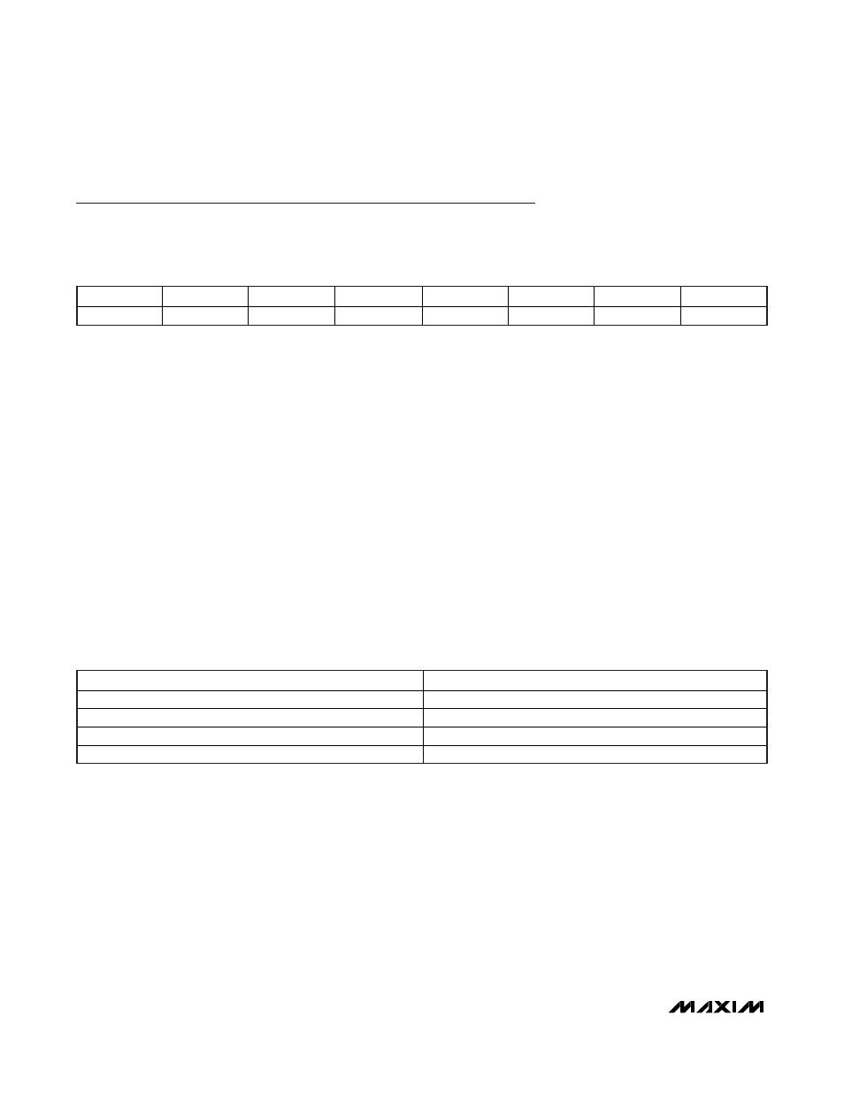
Control Register Format
All Control register bits are read and write accessible. The Control register is recalled from parameter EEPROM
memory at power-up. Register bit values can be modified in shadow RAM after power-up. Power-up default values
are saved by using the Copy Data command.
Control Register (60h)
Bit 7: Negative Blanking Enable (NBEN). A value of 1 enables blanking of negative current values up to 25µV. A
value of 0 disables blanking of negative currents. The power-up default of NBEN = 0.
Bit 6: Undervoltage Enable (UVEN). A value of 1 allows the DS2775–DS2778 to enter sleep mode when the aver-
age of the voltages on V
IN1
and V
IN2
is less than V
UV
and DQ is stable at either logic level for t
SLEEP
. A value of 0
disables transitions to sleep mode during an undervoltage condition.
Bit 5: Power-Mode Enable (PMOD). A value of 1 allows the DS2775–DS2778 to enter sleep mode when DQ is low
for t
SLEEP
. A value of 0 disables DQ-related transitions to sleep mode.
Bit 4: Read Net Address Op Code (RNAOP). A value of 0 selects 33h as the op code value for the Read Net
Address command. A value of 1 selects 39h as the op code value for the Read Net Address command.
Bit 3 and 2: Undervoltage Threshold (VUV[1:0]). Sets the voltage at which the part detects an undervoltage condi-
tion according to Table 4.
Bit 1: Power-Switch PIO Enable (PSPIO). A value of 1 enables the PIO pin as a power-switch input. A value of 0
disables the power-switch input function on PIO pin. This control is independent of the PSDQ state.
Bit 0: Power-Switch DQ Enable (PSDQ). A value of 1 enables the DQ pin as a power-switch input. A value of 0 dis-
ables the power-switch input function on DQ pin. This control is independent of the PSPIO state. This bit has no
effect in the DS2777/DS2778.
DS2775/DS2776/DS2777/DS2778
2-Cell, Stand-Alone, Li+ Fuel-Gauge IC with
Protector and Optional SHA-1 Authentication
26
______________________________________________________________________________________
BIT 7
BIT 6
BIT 5
BIT 4
BIT 3
BIT 2
BIT 1
BIT 0
NBEN UVEN PMOD
RNAOP VUV1 VUV0 PSPIO PSDQ
VUV[1:0] BIT FIELD
V
UV
(V)
00 2.00
01 2.30
10 2.45
11 2.60
Table 4. Undervoltage Threshold