Rainbow Electronics DS2778 User Manual
Page 2
DS2775/DS2776/DS2777/DS2778
2-Cell, Stand-Alone, Li+ Fuel-Gauge IC with
Protector and Optional SHA-1 Authentication
2
_______________________________________________________________________________________
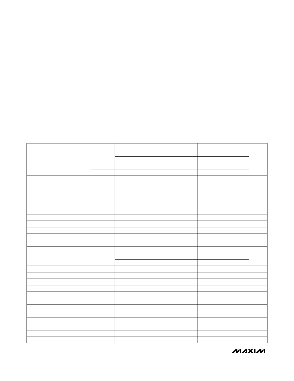
ABSOLUTE MAXIMUM RATINGS
ELECTRICAL CHARACTERISTICS
(V
DD
= +4.0V to +9.2V, T
A
= -20°C to +70°C, unless otherwise noted. Typical values are at T
A
= +25°C.)
Stresses beyond those listed under “Absolute Maximum Ratings” may cause permanent damage to the device. These are stress ratings only, and functional
operation of the device at these or any other conditions beyond those indicated in the operational sections of the specifications is not implied. Exposure to
absolute maximum rating conditions for extended periods may affect device reliability.
Voltage Range on PLS, CP, CC, DC Pins
Relative to V
SS
.....................................................-0.3V to +18V
Voltage Range on V
DD
, V
IN1
, V
IN2
, SRC Pins
Relative to V
SS
....................................................-0.3V to +9.2V
Voltage Range on All Other Pins Relative to V
SS
..-0.3V to +6.0V
Continuous Sink Current, PIO, DQ......................................20mA
Continuous Sink Current, CC, DC.......................................10mA
Operating Temperature Range ...........................-20°C to +70°C
Storage Temperature Range .............................-55°C to +125°C
Soldering Temperature...........................Refer to the IPC/JEDEC
J-STD-020 Specification.
PARAMETER SYMBOL
CONDITIONS
MIN
TYP
MAX
UNITS
Sleep mode, T
A
+50°C
3
5
I
DD0
Sleep mode, T
A
> +50°C
10
I
DD1
Active mode
80
135
Supply Current
I
DD2
Active mode during SHA-1 computation
120
300
μA
Temperature Accuracy
T
ERR
-3
+3
°C
2.0
V
IN1
4.6, 2.0 (V
IN2
- V
IN1
)
4.6,
0°C
T
A
+50°C
-35 +35
2.0
V
IN1
4.6, 2.0 (V
IN2
– V
IN1
)
4.6,
T
A
= +25°C
-22 22
Voltage Accuracy
2.0
V
IN1
4.6, 2.0 (V
IN2
- V
IN1
)
4.6
-50
+50
mV
Input Resistance (V
IN1
, V
IN2
)
15
M
Current Resolution
I
LSB
1.56
μV
Current Full Scale
I
FS
-51.2
+51.2
mV
Current Gain Error
I
GERR
-1
+1
%
FS
Current Offset
I
OERR
0°C
T
A
+70°C (Note 1)
-9.375
9.375
μVh
Accumulated Current Offset
q
OERR
0°C
T
A
+70°C (Note 1)
-255
0
μVh/Day
0°C
T
A
+50°C
-2
+2
Time-Base Error
t
ERR
-3
+3
%
CP Output Voltage (V
CP
- V
SRC
) V
GS
I
OUT
= 0.9μA
4.4
4.7
5
V
CP Startup Time
t
SCP
CE = 0, DE = 0, C
CP
= 0.1μF, active mode
200
ms
Output High: CC, DC
V
OHCP
I
OH
= 100μA (Note 2)
V
CP
- 0.4
V
Output Low: CC
V
OLCC
I
OL
= 100μA
V
SRC
+ 0.1
V
Output Low: DC
V
OLDC
I
OL
= 100μA
V
SRC
+ 0.1
V
DQ, PIO Voltage Range
-0.3
+5.5
V
DQ, PIO, SDA, SCL Input
Logic-High
V
IH
1.5
V
DQ, PIO, SDA, SCL Input
Logic-Low
V
IL
0.6
V
OVD Input Logic-High
V
IH
V
BAT
- 0.2
V
OVD Input Logic-Low
V
IL
V
SS
+ 0.2
V