Rainbow Electronics DS2778 User Manual
Page 5
DS2775/DS2776/DS2777/DS2778
2-Cell, Stand-Alone, Li+ Fuel-Gauge IC with
Protector and Optional SHA-1 Authentication
_______________________________________________________________________________________
5
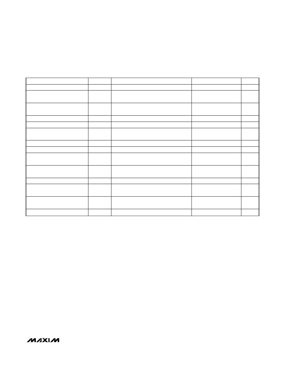
ELECTRICAL CHARACTERISTICS: 2-WIRE INTERFACE (DS2777/DS2778 ONLY)
(V
DD
= +4.0V to +9.2V, T
A
= -20°C to +70°C.)
PARAMETER SYMBOL
CONDITIONS
MIN
TYP
MAX
UNITS
SCL Clock Frequency
f
SCL
(Note
4)
0
400 kHz
Bus-Free Time Between a STOP
and START Condition
t
BUF
1.3
μs
Hold Time (Repeated) START
Condition
t
HD:STA
(Note
5)
0.6
μs
Low Period of SCL Clock
t
LOW
1.3
μs
High Period of SCL Clock
t
HIGH
0.6
μs
Setup Time for a Repeated
START Condition
t
SU:STA
0.6
μs
Data Hold Time
t
HD:DAT
(Notes 6, 7)
0
0.9
μs
Data Setup Time
t
SU:DAT
(Note
6)
100
ns
Rise Time of Both SDA and SCL
Signals
t
R
20 +
0.1C
B
300 ns
Fall Time of Both SDA and SCL
Signals
t
F
20 +
0.1C
B
300 ns
Setup Time for STOP Condition
t
SU:STO
0.6
μs
Spike Pulse Widths Suppressed
by Input Filter
t
SP
(Note
8)
0
50 ns
Capacitive Load for Each Bus
Line
C
B
(Note
9)
400 pF
SCL, SDA Input Capacitance
C
BIN
60
pF
Note 1: Accumulation bias and offset bias registers set to 00h. NBEN bit set to 0.
Note 2: Measurement made with V
SRC
= +8V, V
GS
driven with external +4.5V supply.
Note 3: Overvoltage (OV) and undervoltage (UV) delays (t
OVD
, t
UVD
) are reduced to zero seconds if the OV or UV condition is
detected within 100ms of entering active mode.
Note 4: Timing must be fast enough to prevent the DS2777/DS2778 from entering sleep mode due to bus low for period > t
SLEEP
.
Note 5: f
SCL
must meet the minimum clock low time plus the rise/fall times.
Note 6: The maximum t
HD:DAT
need only be met if the device does not stretch the low period (t
LOW
) of the SCL signal.
Note 7: This device internally provides a hold time of at least 75ns for the SDA signal (referred to the V
IHMIN
of the SCL signal) to
bridge the undefined region of the falling edge of SCL.
Note 8: Filters on SDA and SCL suppress noise spikes at the input buffers and delay the sampling instant.
Note 9: C
B
is total capacitance of one bus line in pF.