5 program and erase characteristics, 6 power-up conditions, 7 input test waveforms and measurement levels – Rainbow Electronics AT25DF081 User Manual
Page 30: 8 output test load
30
3674E–DFLASH–8/08
AT25DF081
Notes:
1. Not 100% tested (value guaranteed by design and characterization).
12.7
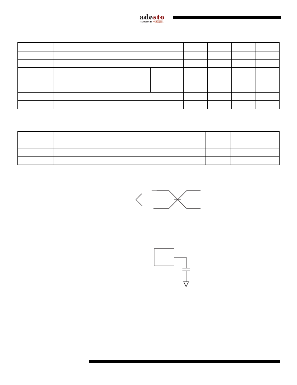
Input Test Waveforms and Measurement Levels
12.8
Output Test Load
12.5
Program and Erase Characteristics
Symbol
Parameter
Min
Typ
Max
Units
t
PP
Page Program Time (256 Bytes)
1.0
5.0
ms
t
BP
Byte Program Time
15
µs
t
BLKE
Block Erase Time
4-Kbyte
50
200
ms
32-Kbyte
350
600
64-Kbyte
600
950
t
CHPE
Chip Erase Time
8
14
sec
t
WRSR
Write Status Register Time
200
ns
12.6
Power-Up Conditions
Symbol
Parameter
Min
Max
Units
t
VCSL
Minimum V
CC
to Chip Select Low Time
70
µs
t
PUW
Power-up Device Delay Before Program or Erase Allowed
10
ms
V
POR
Power-On Reset Voltage
0.9
1.1
V
AC
DRIVING
LEVELS
AC
MEASUREMENT
LEVEL
0.1V
CC
V
CC
/2
0.9V
CC
t
R
, t
F
< 2 ns (10% to 90%)
DEVICE
UNDER
TEST
30 pF
See also other documents in the category Rainbow Electronics Storage:
- W27E010 (14 pages)
- W27L520 (16 pages)
- W29EE512 (21 pages)
- W27E512 (16 pages)
- W24100 (11 pages)
- W27E040 (15 pages)
- W25Q32 (60 pages)
- W49L102 (21 pages)
- W29C040 (20 pages)
- W29EE011 (20 pages)
- W49F020 (21 pages)
- W2465 (10 pages)
- W24256 (10 pages)
- W982516CH (43 pages)
- MAX16014 (12 pages)
- W24512A (10 pages)
- W27E020 (14 pages)
- W29C020C (21 pages)
- W25X64 (47 pages)
- W24257 (11 pages)
- W24L257 (10 pages)
- W9864G2GH (48 pages)
- W24L11 (11 pages)
- W27L010 (14 pages)
- W27E520 (16 pages)
- W27LE520 (16 pages)
- W9825G6CH (43 pages)
- W49F002U (23 pages)
- W9864G6GB (47 pages)
- AT45DB011B (32 pages)
- AT45DB642 (71 pages)
- AT45DB642 (37 pages)
- AT45DB161D (51 pages)
- AT27LV040A (12 pages)
- AT29LV010A (15 pages)
- HT24LC08 (11 pages)
- AT29C257 (12 pages)
- AT45DB161B (32 pages)
- AT27C1024 (12 pages)
- AT28BV256 (12 pages)
- AT28C040 (12 pages)
- DS1258Y_AB (9 pages)
- AT28BV64B (12 pages)
- AT27C512R (12 pages)
- DS1220AB_AD (9 pages)