Switching considerations, Block diagram – Rainbow Electronics AT27C040 User Manual
Page 2
AT27C040
2
Atmel’s scaled CMOS technology provides low active
power consumption, and fast programming. Power con-
sumption is typically 8 mA in active mode and less than
10
µ
A in standby mode.
The AT27C040 is available in a choice of industry standard
JEDEC-approved one-time programmable (OTP) plastic
PDIP, PLCC, SOIC (SOP), and TSOP packages. The
device features two-line control (CE, OE) to eliminate bus
contention in high-speed systems.
Atmel’s AT27C040 has additional features to ensure high
quality and efficient production use. The Rapid
™
Program-
ming Algorithm reduces the time required to program the
part and guarantees reliable programming. Programming
time is typically only 100
µ
s/byte. The Integrated Product
Identification Code electronically identifies the device and
manufacturer. This feature is used by industry standard
programming equipment to select the proper programming
algorithms and voltages.
Switching Considerations
Switching between active and standby conditions via the
Chip Enable pin may produce transient voltage excursions.
Unless accommodated by the system design, these tran-
sients may exceed data sheet limits, resulting in device
non-conformance. At a minimum, a 0.1
µ
F high frequency,
low inherent inductance, ceramic capacitor should be uti-
lized for each device. This capacitor should be connected
between the V
CC
and Ground terminals of the device, as
close to the device as possible. Additionally, to stabilize the
supply voltage level on printed circuit boards with large
EPROM arrays, a 4.7
µ
F bulk electrolytic capacitor should
be utilized, again connected between the V
CC
and Ground
terminals. This capacitor should be positioned as close as
possible to the point where the power supply is connected
to the array.
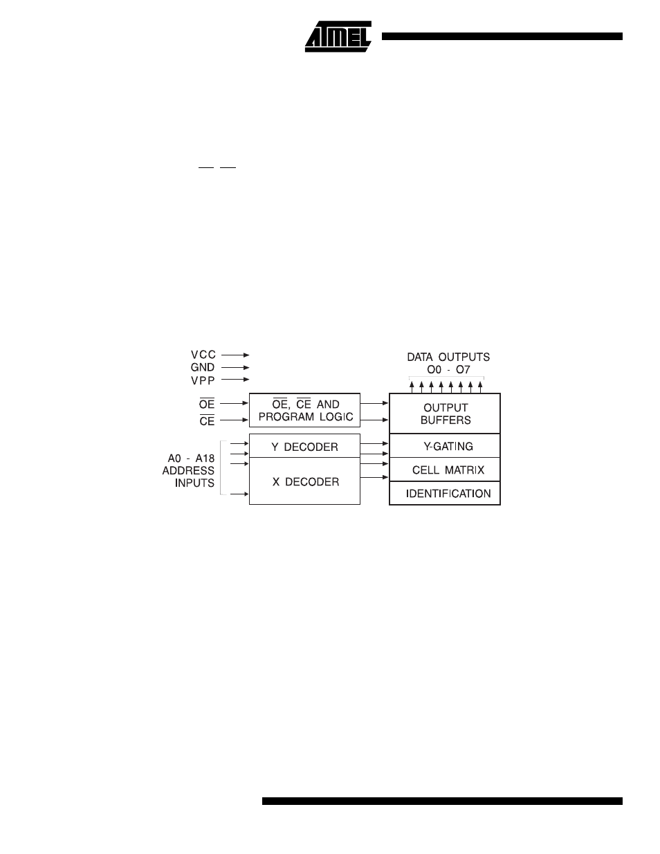
Block Diagram