Rainbow Electronics AT27C040 User Manual
Features, Description, Pin configurations

1
4-Megabit
(512K x 8)
OTP EPROM
AT27C040
Features
•
Fast Read Access Time - 70 ns
•
Low Power CMOS Operation
– 100
µA max. Standby
– 30 mA max. Active at 5 MHz
•
JEDEC Standard Packages
– 32-Lead 600-mil PDIP
– 32-Lead 450-mil SOIC (SOP)
– 32-Lead PLCC
– 32-Lead TSOP
•
5V
±
10% Supply
•
High Reliability CMOS Technology
– 2000V ESD Protection
– 200 mA Latchup Immunity
•
Rapid™ Programming Algorithm - 100 µs/byte (typical)
•
CMOS and TTL Compatible Inputs and Outputs
•
Integrated Product Identification Code
•
Commercial and Industrial Temperature Ranges
Description
The AT27C040 chip is a low-power, high-performance, 4,194,304-bit one-time pro-
grammable read only memory (OTP EPROM) organized as 512K by 8 bits. The
AT27C040 requires only one 5V power supply in normal read mode operation. Any
byte can be accessed in less than 70 ns, eliminating the need for speed reducing
WAIT states on high-performance microprocessor systems.
Rev. 0189E–07/97
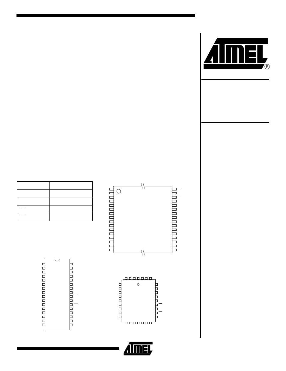
Pin Configurations
Pin Name
Function
A0 - A18
Addresses
O0 - O7
Outputs
CE
Chip Enable
OE
Output Enable
PDIP, SOIC Top View
1
2
3
4
5
6
7
8
9
10
11
12
13
14
15
16
32
31
30
29
28
27
26
25
24
23
22
21
20
19
18
17
VPP
A16
A15
A12
A7
A6
A5
A4
A3
A2
A1
A0
O0
O1
O2
GND
VCC
A18
A17
A14
A13
A8
A9
A11
OE
A10
CE
07
06
05
04
03
TSOP Top View
1
2
3
4
5
6
7
8
9
10
11
12
13
14
15
16
32
31
30
29
28
27
26
25
24
23
22
21
20
19
18
17
A11
A9
A8
A13
A14
A17
A18
VCC
VPP
A16
A15
A12
A7
A6
A5
A4
OE
A10
CE
07
06
05
04
03
GND
02
01
O0
A0
A1
A2
A3
PLCC Top View
5
6
7
8
9
10
11
12
13
29
28
27
26
25
24
23
22
21
A7
A6
A5
A4
A3
A2
A1
A0
O0
A14
A13
A8
A9
A11
OE
A10
CE
07
4
3
2
1
32
31
30
14
15
16
17
18
19
20
01
02
GND
03
04
05
06
A12
A15
A16
VPP
VCC
A18
A17
(continued)
