Ac timing characteristics – 3.3v operation at40klv, At40k/at40klv series fpga – Rainbow Electronics AT40K40LV User Manual
Page 35
35
AT40K/AT40KLV Series FPGA
0896C–FPGA–04/02
AC Timing Characteristics – 3.3V Operation AT40KLV
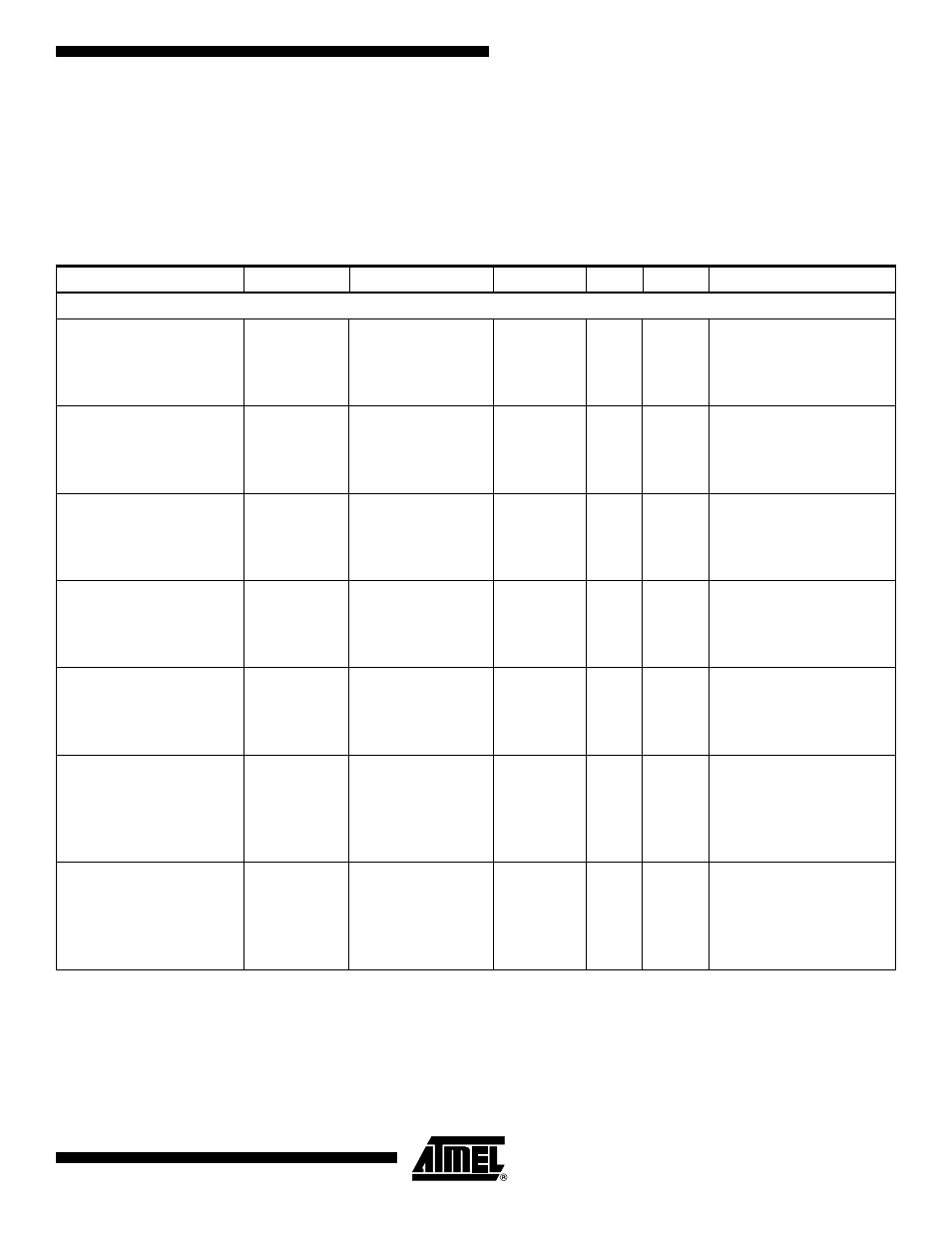
Delays are based on fixed loads and are described in the notes.
Maximum times based on worst case: V
CC
= 3.0V, temperature = 70
°C
Minimum times based on best case: V
CC
= 3.6V, temperature = 0
°C
Maximum delays are the average of t
PDLH
and t
PDHL
.
Clocks and Reset Input buffers are measured from a V
IH
of 1.5V at the input pad to the internal V
IH
of 50% of V
CC
.
Maximum times for clock input buffers and internal drivers are measured for rising edge delays only.
Cell Function
Parameter
Path
Device
-3
Units
Notes
Global Clocks and Set/Reset
GCK Input Buffer
t
PD
(Maximum)
pad -> clock
pad -> clock
pad -> clock
pad -> clock
AT40K05LV
AT40K10LV
AT40K20LV
AT40K40LV
1.3
1.5
1.6
1.9
ns
ns
ns
ns
Rising edge clock
FCK Input Buffer
t
PD
(Maximum)
pad -> clock
pad -> clock
pad -> clock
pad -> clock
AT40K05LV
AT40K10LV
AT40K20LV
AT40K40LV
0.7
0.8
0.8
0.9
ns
ns
ns
ns
Rising edge clock
Clock Column Driver
t
PD
(Maximum)
clock -> colclk
clock -> colclk
clock -> colclk
clock -> colclk
AT40K05LV
AT40K10LV
AT40K20LV
AT40K40LV
1.5
1.8
2.0
2.5
ns
ns
ns
ns
Rising edge clock
Clock Sector Driver
t
PD
(Maximum)
colclk -> secclk
colclk -> secclk
colclk -> secclk
colclk -> secclk
AT40K05LV
AT40K10LV
AT40K20LV
AT40K40LV
1.0
1.0
1.0
1.0
ns
ns
ns
ns
Rising edge clock
GSRN Input Buffer
t
PD
(Maximum)
pad -> GSRN
pad -> GSRN
pad -> GSRN
pad -> GSRN
AT40K05LV
AT40K10LV
AT40K20LV
AT40K40LV
4.5
5.4
6.3
8.2
ns
ns
ns
ns
Global Clock to Output
t
PD
(Maximum)
clock pad -> out
clock pad -> out
clock pad -> out
clock pad -> out
AT40K05LV
AT40K10LV
AT40K20LV
AT40K40LV
13.0
13.4
13.8
14.5
ns
ns
ns
ns
Rising edge clock
Fully loaded clock tree
Rising edge DFF
20 mA output buffer
50 pf pin load
Fast Clock to Output
t
PD
(Maximum)
clock pad -> out
clock pad -> out
clock pad -> out
clock pad -> out
AT40K05LV
AT40K10LV
AT40K20LV
AT40K40LV
12.4
12.7
13.0
13.5
ns
ns
ns
ns
Rising edge clock
Fully loaded clock tree
Rising edge DFF
20 mA output buffer
50 pf pin load