At40k/at40klv series fpga – Rainbow Electronics AT40K40LV User Manual
Page 12
12
AT40K/AT40KLV Series FPGA
0896C–FPGA–04/02
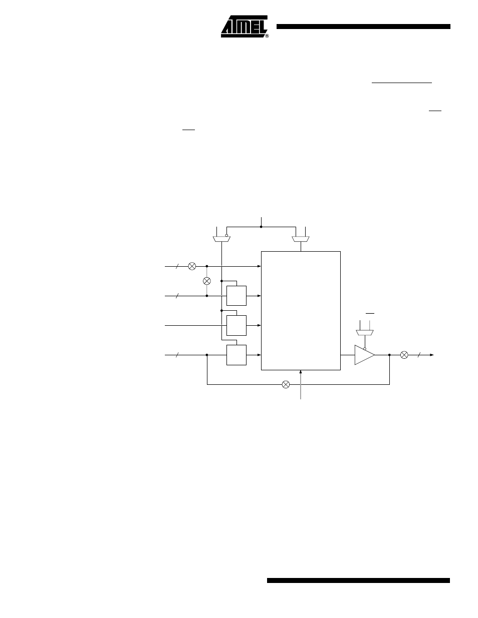
Reading and writing of the 10 ns 32 x 4 dual-port FreeRAM are independent of each
other. Reading the 32 x 4 dual-port RAM is completely asynchronous. Latches are
transparent; when Load is logic 1, data flows through; when Load is logic 0, data is
latched. These latches are used to synchronize Write Address, Write Enable Not, and
Din signals for a synchronous RAM. Each bit in the 32 x 4 dual-port RAM is also a trans-
parent latch. The front-end latch and the memory latch together form an edge-triggered
flip flop. When a nibble (bit = 7) is (Write) addressed and LOAD is logic 1 and WE is
logic 0, data flows through the bit. When a nibble is not (Write) addressed or LOAD is
logic 0 or WE is logic 1, data is latched in the nibble. The two CLOCK muxes are con-
trolled together; they both select CLOCK (for a synchronous RAM) or they both select
“1” (for an asynchronous RAM). CLOCK is obtained from the clock for the sector-column
immediately to the left and immediately above the RAM block. Writing any value to the
RAM clear byte during configuration clears the RAM (see the “
AT40K Configuration
Series” application note at www.atmel.com).
Figure 8. RAM Logic
Figure 9 on page 13 shows an example of a RAM macro constructed using the
AT40K/AT40KLV’s FreeRAM cells. The macro shown is a 128 x 8 dual-ported asyn-
chronous RAM. Note the very small amount of external logic required to complete the
address decoding for the macro. Most of the logic cells (core cells) in the sectors occu-
pied by the RAM will be unused: they can be used for other logic in the design. This
logic can be automatically generated using the macro generators.
Write Address
Din
Dout
Read Address
“1”
“1”
Write Enable NOT
RAM-Clear Byte
Dout
0
1
0
1
“1”
CLOCK
Load
5
Ain
Aout
WEN
Din
Load
Latch
Load
Latch
Load
Latch
Clear
32 x 4
Dual-port
RAM
OE
4
4
5