Rainbow Electronics AT45DB021B User Manual
Megabit 2.7-volt only dataflash, Features, Description
1
Features
•
Single 2.7V - 3.6V Supply
•
Serial Peripheral Interface (SPI) Compatible
•
Page Program Operation
– Single Cycle Reprogram (Erase and Program)
– 1024 Pages (264 Bytes/Page) Main Memory
•
Supports Page and Block Erase Operations
•
Two 264-byte SRAM Data Buffers – Allows Receiving of Data
while Reprogramming of Nonvolatile Memory
•
Continuous Read Capability through Entire Array
– Ideal for Code Shadowing Applications
•
Low Power Dissipation
– 4 mA Active Read Current Typical
– 2 µA CMOS Standby Current Typical
•
20 MHz Max Clock Frequency
•
Hardware Data Protection Feature
•
100% Compatible to AT45DB021 and AT45DB021A
•
5.0V-tolerant Inputs: SI, SCK, CS, RESET and WP Pins
•
Commercial and Industrial Temperature Ranges
Description
The AT45DB021B is a 2.7-volt only, serial interface Flash memory ideally suited for
a wide variety of digital voice-, image-, program code- and data-storage applications.
Its 2,162,688 bits of memory are organized as 1024 pages of 264 bytes each. In addi-
tion to the main memory, the AT45DB021B also contains two SRAM data buffers
of 264 bytes each. The buffers allow receiving of data while a page in the main mem-
ory is being reprogrammed, as well as reading or writing a continuous data stream.
2-megabit
2.7-volt Only
DataFlash
®
AT45DB021B
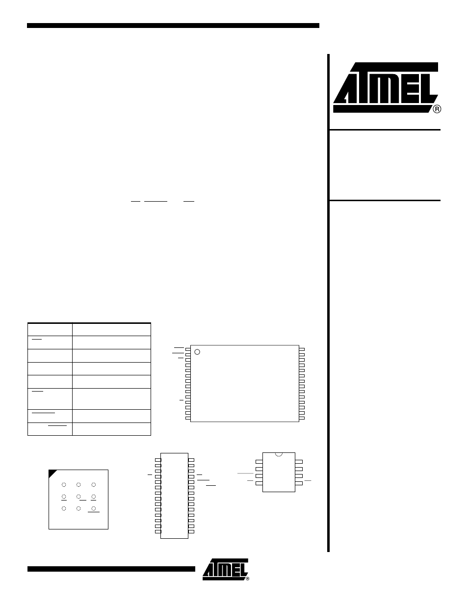
Pin Configurations
Pin Name
Function
CS
Chip Select
SCK
Serial Clock
SI
Serial Input
SO
Serial Output
WP
Hardware Page Write
Protect Pin
RESET
Chip Reset
RDY/BUSY
Ready/Busy
CBGA Top View
through Package
A
B
C
1
2
3
VCC
WP
RESET
GND
RDY/BSY
SI
SCK
CS
SO
TSOP Top View
Type 1
1
2
3
4
5
6
7
8
9
10
11
12
13
14
28
27
26
25
24
23
22
21
20
19
18
17
16
15
RDY/BUSY
RESET
WP
NC
NC
VCC
GND
NC
NC
NC
CS
SCK
SI
SO
NC
NC
NC
NC
NC
NC
NC
NC
NC
NC
NC
NC
NC
NC
28-SOIC
1
2
3
4
5
6
7
8
9
10
11
12
13
14
28
27
26
25
24
23
22
21
20
19
18
17
16
15
GND
NC
NC
CS
SCK
SI
SO
NC
NC
NC
NC
NC
NC
NC
VCC
NC
NC
WP
RESET
RDY/BUSY
NC
NC
NC
NC
NC
NC
NC
NC
8-SOIC
1
2
3
4
8
7
6
5
SI
SCK
RESET
CS
SO
GND
VCC
WP
Rev. 1937F–DFLSH–10/02
Document Outline
- Pin Configurations
- Features
- Description
- Block Diagram
- Memory Array
- Memory Architecture Diagram
- Device Operation
- Status Register Format
- Block Erase Addressing
- Power-on/Reset State
- Absolute Maximum Ratings*
- DC and AC Operating Range
- DC Characteristics
- AC Characteristics
- Input Test Waveforms and Measurement Levels
- Output Test Load
- AC Waveforms
- Write Operations
- Read Operations
- Detailed Bit-level Read Timing – Inactive Clock Polarity Low
- Detailed Bit-level Read Timing – Inactive Clock Polarity Low (Continued)
- Detailed Bit-level Read Timing – Inactive Clock Polarity High
- Detailed Bit-level Read Timing – Inactive Clock Polarity High (Continued)
- Detailed Bit-level Read Timing – SPI Mode 0
- Detailed Bit-level Read Timing – SPI Mode 0 (Continued)
- Detailed Bit-level Read Timing – SPI Mode 3
- Detailed Bit-level Read Timing – SPI Mode 3 (Continued)
- Sector Addressing
- Packaging Information