Pin description, Memory organization, Pin capacitance – Rainbow Electronics AT24C01 User Manual
Page 3: Dc characteristics, At24c01
3
AT24C01
0134E–SEEPR–08/02
Pin Description
SERIAL CLOCK (SCL): The SCL input is used to positive edge clock data into each
EEPROM device and negative edge clock data out of each device.
SERIAL DATA (SDA): The SDA pin is bidirectional for serial data transfer. This pin is
open-drain driven and may be wire-ORed with any number of other open-drain or open
collector devices.
Memory Organization
AT24C01, 1K SERIAL EEPROM: Internally organized with 128 pages of 1 byte each.
The 1K requires a 7-bit data word address for random word addressing.
Note:
1. V
IL
min and V
IH
max are reference only and are not tested.
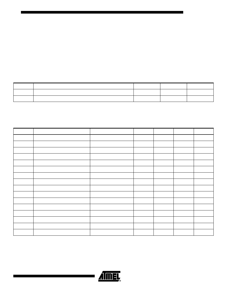
Pin Capacitance
Applicable over recommended operating range from T
A
= 25
°C, f = 1.0 MHz, V
CC
= +1.8V.
Symbol
Test Condition
Max
Units
Condition
C
I/O
Input/Output Capacitance (SDA)
8
pF
V
I/O
= 0V
C
IN
Input Capacitance (A0, A1, A2, SCL)
6
pF
V
IN
= 0V
DC Characteristics
Applicable over recommended operating range from: T
AI
= -40
°C to +85°C, V
CC
= +1.8V to +5.5V, T
AC
= 0
°C to +70°C,
V
CC
= +1.8V to +5.5V (unless otherwise noted).
Symbol
Parameter
Test Condition
Min
Typ
Max
Units
V
CC1
Supply Voltage
1.8
5.5
V
V
CC2
Supply Voltage
2.5
5.5
V
V
CC3
Supply Voltage
2.7
5.5
V
V
CC4
Supply Voltage
4.5
5.5
V
I
CC
Supply Current V
CC
= 5.0V
READ at 100 kHz
0.4
1.0
mA
I
CC
Supply Current V
CC
= 5.0V
WRITE at 100 kHz
2.0
3.0
mA
I
SB1
Standby Current V
CC
= 1.8V
V
IN
= V
CC
or V
SS
0.6
3.0
µA
I
SB2
Standby Current V
CC
= 2.5V
V
IN
= V
CC
or V
SS
1.4
4.0
µA
I
SB3
Standby Current V
CC
= 2.7V
V
IN
= V
CC
or V
SS
1.6
4.0
µA
I
SB4
Standby Current V
CC
= 5.0V
V
IN
= V
CC
or V
SS
8.0
18.0
µA
I
LI
Input Leakage Current
V
IN
= V
CC
or V
SS
0.10
3.0
µA
I
LO
Output Leakage Current
V
OUT
= V
CC
or V
SS
0.05
3.0
µA
V
IL
Input Low Level
(1)
-0.6
V
CC
× 0.3
V
V
IH
Input High Level
(1)
V
CC
× 0.7
V
CC
+ 0.5
V
V
OL2
Output Low Level V
CC
= 3.0V
I
OL
= 2.1 mA
0.4
V
V
OL1
Output Low Level V
CC
= 1.8V
I
OL
= 0.15 mA
0.2
V