Rainbow Electronics BR24L01AFVM-W User Manual
Page 20
BR24L01A-W / BR24L01AF-W / BR24L01AFJ-W /
Memory ICs
BR24L01AFV-W / BR24L01AFVM-W
20/25
8) Notes for noise on V
CC
•
About bypass capacitor
Noise and surges on power line may cause the abnormal function. It is recommended that the bypass capacitors
(0.1
µ
F) are attached on the V
CC
and GND line beside the device.
The attachment of bypass capacitors on the board near by connector is also recommended.
GND
V
CC
PRINT BASE
IC
capacitor 0.01 to 0.1
µ
F
capacitor 10 to 100
µ
F
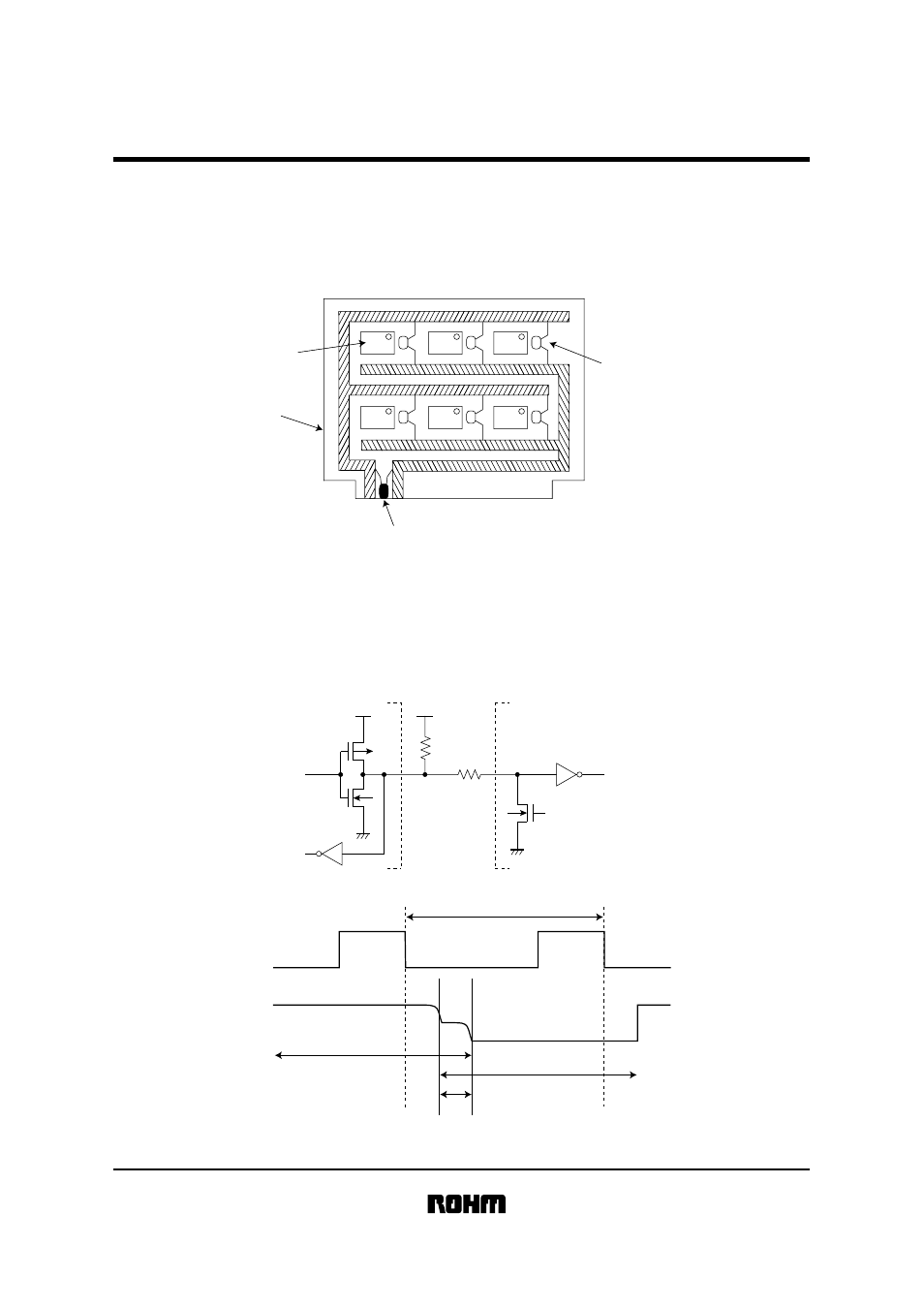
9) The notice about the connection of controller
•
About R
S
The open drain interface is recommended for SDA port in I
2
CBUS. But, in the case that Tri-state CMOS interface is
applied to SDA, insert a series resister R
S
between SDA pin of the device and a pull up resister R
PU
. It limits the
current from PMOS of controller to NMOS of EEPROM.
R
S
also protects SDA pin from surges. Therefore, R
S
is able to be used though SDA port is open drain.
R
PU
R
S
CONTROLLER
EEPROM
"H" OUTPUT OF
CONTROLLER
"L" OUTPUT OF
EEPROM
ACK
SCL
SDA
The "H" output of controller
and the "L" output of EEPROM may cause
current overload to SDA line.