Rainbow Electronics BR24L01AFVM-W User Manual
Page 10
BR24L01A-W / BR24L01AF-W / BR24L01AFJ-W /
Memory ICs
BR24L01AFV-W / BR24L01AFVM-W
10/25
zByte write
SDA
LINE
WP
S
T
A
R
T
SLAVE
ADDRESS
1 0
0
1
R
/
W
W
R
I
T
E
A
C
K
A
C
K
D7
DATA
D0
S
T
O
P
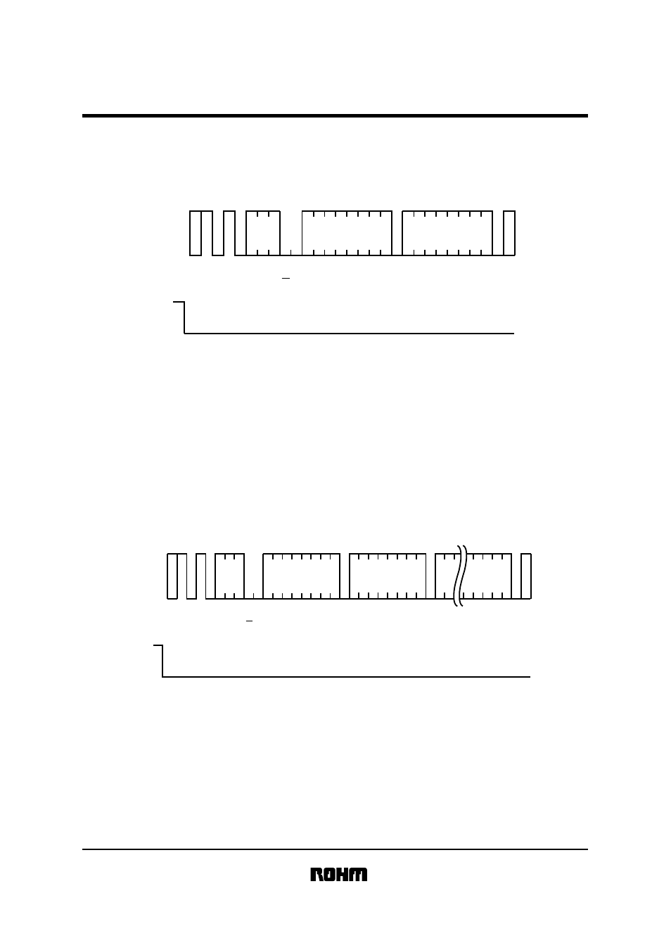
Fig.8 BYTE WRITE CYCLE TIMING
A
C
K
WORD
ADDRESS
WA
0
WA
6
∗
A0
A1
A2
•
By using this command, the data is programmed into the indicated word address.
•
When the master generates a STOP condition, the device begins the internal write cycle to the nonvolatile memory
array.
zPage write
Fig.9 PAGE WRITE CYCLE TIMING
SDA
LINE
WP
S
T
A
R
T
SLAVE
ADDRESS
1 0
0
1
R
/
W
W
R
I
T
E
A
C
K
A
C
K
A
C
K
D7
DATA (n)
D0
DATA (n+7)
D0
S
T
O
P
A
C
K
WORD
ADDRESS (n)
WA
0
WA
6
∗
A0
A1
A2
•
This device is capable of eight byte page write operation.
•
When two or more byte data are inputted, the three low order address bits are internally incremented by one after the
receipt of each word. The four higher order bits of the address (WA6 to WA3) remain constant.
•
If the master transmits more than eight words, prior to generating the STOP condition, the address counter will
“roll over”, and the previous transmitted data will be overwritten.