Rainbow Electronics ATtiny12 User Manual
Features, Pin configuration
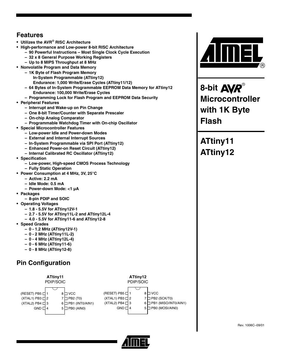
Table of contents
Document Outline
- Features
- Pin Configuration
- Description
- Architectural Overview
- General-purpose Register File
- ALU – Arithmetic Logic Unit
- Flash Program Memory
- Program and Data Addressing Modes
- Subroutine and Interrupt Hardware Stack
- EEPROM Data Memory
- Memory Access and Instruction Execution Timing
- I/O Memory
- Reset and Interrupt Handling
- ATtiny12 Internal Voltage Reference
- Interrupt Handling
- Sleep Modes for the ATtiny11
- Sleep Modes for the ATtiny12
- ATtiny12 Calibrated Internal RC Oscillator
- Timer/Counter0
- Watchdog Timer
- ATtiny12 EEPROM Read/Write Access
- Analog Comparator
- I/O Port B
- Memory Programming
- Program (and Data) Memory Lock Bits
- Fuse Bits in ATtiny11
- Fuse Bits in ATtiny12
- Signature Bytes
- Calibration Byte in ATtiny12
- Programming the Flash and EEPROM
- High-voltage Serial Programming
- High-voltage Serial Programming Algorithm
- High-voltage Serial Programming Characteristics
- Low-voltage Serial Downloading (ATtiny12 only)
- Low-voltage Serial Programming Characteristics
- Electrical Characteristics
- Register Summary ATtiny11
- Register Summary ATtiny12
- Instruction Set Summary
- Ordering Information
- Packaging Information