Port b data register – portb, Port b data direction register – ddrb, Port b input pins address – pinb – Rainbow Electronics ATtiny12 User Manual
Page 42: Port b as general digital i/o, Attiny11/12, Table 20. ddbn effects on port b pins
42
ATtiny11/12
1006C–09/01
Port B Data Register – PORTB
Port B Data Direction Register
– DDRB
Note:
DDB5 is only available in ATtiny12.
Port B Input Pins Address –
PINB
The Port B Input Pins address – PINB – is not a register, and this address enables
access to the physical value on each Port B pin. When reading PORTB, the Port B Data
Latch is read, and when reading PINB, the logical values present on the pins are read.
Port B as General Digital I/O
The lowermost five pins in port B have equal functionality when used as digital I/O pins.
PBn, General I/O pin: The DDBn bit in the DDRB register selects the direction of this
pin, if DDBn is set (one), PBn is configured as an output pin. If DDBn is cleared (zero),
PBn is configured as an input pin. If PORTBn is set (one) when the pin is configured as
an input pin, the MOS pull-up resistor is activated. On ATtiny12 this feature can be dis-
abled by setting the Pull-up Disable (PUD) bit in the MCUCR register. To switch the pull-
up resistor off, the PORTBn can be cleared (zero), the pin can be configured as an out-
put pin, or in ATtiny12, the PUD bit can be set. The port pins are tri-stated when a reset
condition becomes active, even if the clock is not running.
n: 4,3…0, pin number.
Note that in ATtiny11, PB5 is input only. On ATtiny12, PB5 is input or open-drain output.
Because this pin is used for 12V programming, there is no ESD protection diode limiting
the voltage on the pin to V
CC
+ 0.5V. Thus, special care should be taken to ensure that
the voltage on this pin does not rise above V
CC
+ 1V during normal operation. This may
cause the MCU to reset or enter programming mode unintentionally.
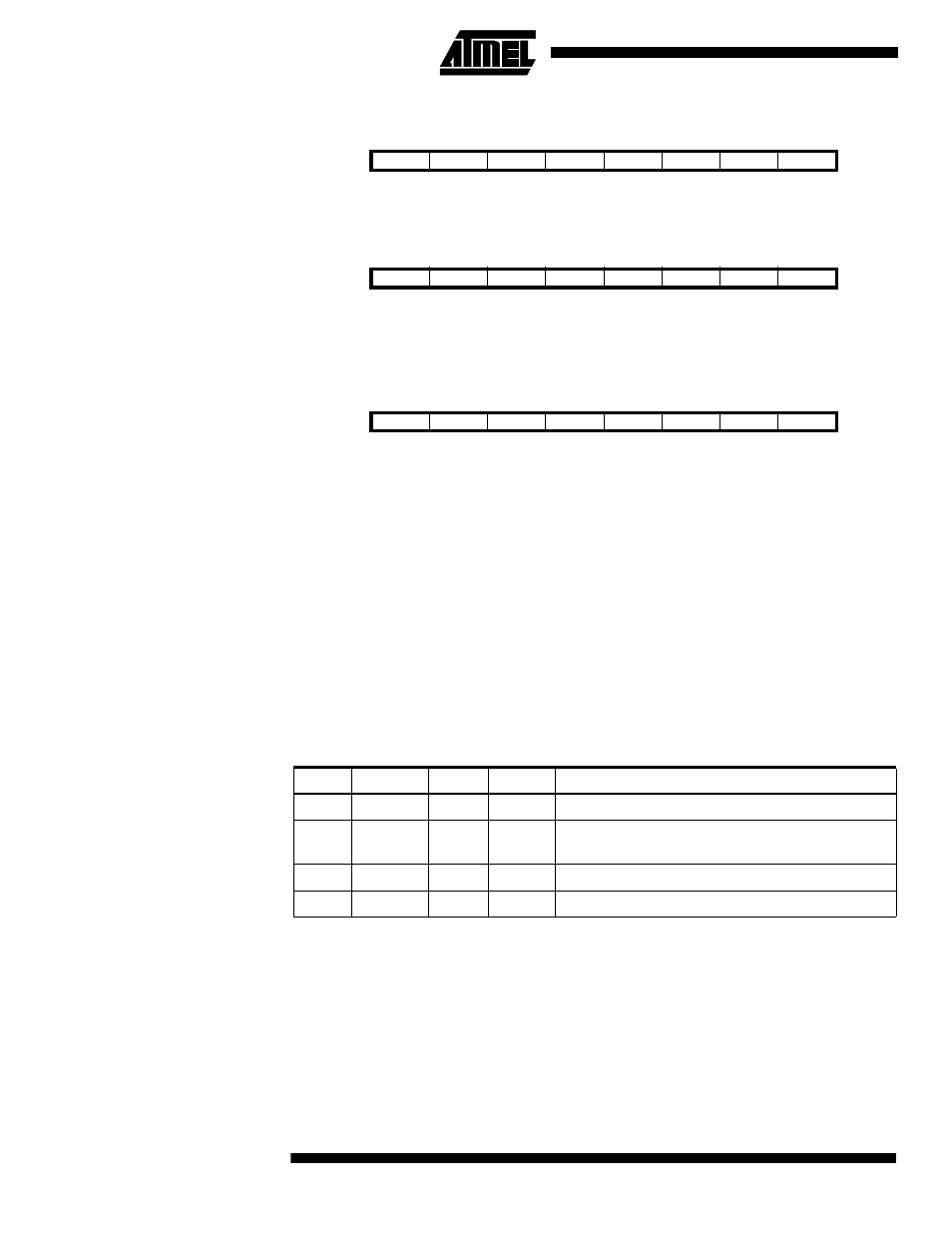
Bit
7
6
5
4
3
2
1
0
$18
-
-
-
PORTB4
PORTB3
PORTB2
PORTB1
PORTB0
PORTB
Read/Write
R
R
R
R/W
R/W
R/W
R/W
R/W
Initial Value
0
0
0
0
0
0
0
0
Bit
7
6
5
4
3
2
1
0
$17
-
-
(DDB5)
DDB4
DDB3
DDB2
DDB1
DDB0
DDRB
Read/Write
R
R
R(/W)
R/W
R/W
R/W
R/W
R/W
Initial Value
0
0
0
0
0
0
0
0
Bit
7
6
5
4
3
2
1
0
$16
-
-
PINB5
PINB4
PINB3
PINB2
PINB1
PINB0
PINB
Read/Write
R
R
R
R
R
R
R
R
Initial Value
0
0
N/A
N/A
N/A
N/A
N/A
N/A
Table 20. DDBn Effects on Port B Pins
DDBn
PORTBn
I/O
Pull-up
Comment
0
0
Input
No
Tri-state (Hi-Z)
0
1
Input
Yes
PBn will source current if ext. pulled low. In ATtiny12
pull-ups can be disabled by setting the PUD bit.
1
0
Output
No
Push-pull Zero Output
1
1
Output
No
Push-pull One Output