Attiny12 block diagram, Attiny11/12 – Rainbow Electronics ATtiny12 User Manual
Page 4
4
ATtiny11/12
1006C–09/01
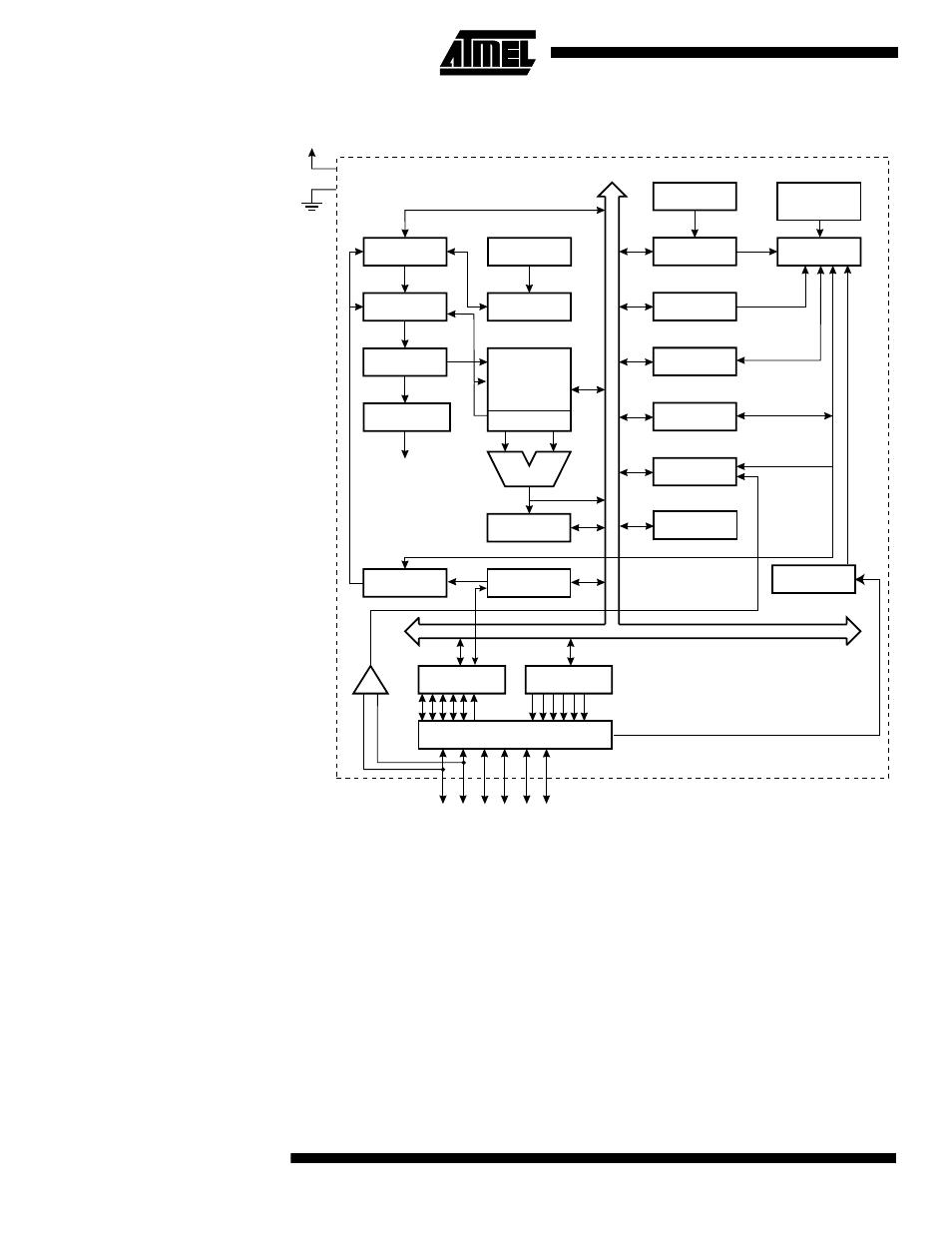
ATtiny12 Block Diagram
Figure 2. The ATtiny12 Block Diagram
The ATtiny12 provides the following features: 1K bytes of Flash, 64 bytes EEPROM, up
to six general-purpose I/O lines, 32 general-purpose working registers, an 8-bit
timer/counter, internal and external interrupts, programmable Watchdog Timer with
internal oscillator, and two software-selectable power-saving modes. The Idle Mode
stops the CPU while allowing the timer/counters and interrupt system to continue func-
tioning. The Power-down Mode saves the register contents but freezes the oscillator,
disabling all other chip functions until the next interrupt or hardware reset. The wake-up
or interrupt on pin change features enable the ATtiny12 to be highly responsive to exter-
nal events, still featuring the lowest power consumption while in the power-down modes.
The device is manufactured using Atmel’s high-density nonvolatile memory technology.
By combining an RISC 8-bit CPU with Flash on a monolithic chip, the Atmel ATtiny12 is
a powerful microcontroller that provides a highly-flexible and cost-effective solution to
many embedded control applications.
PROGRAM
COUNTER
INTERNAL
OSCILLATOR
WATCHDOG
TIMER
STACK
POINTER
PROGRAM
FLASH
HARDWARE
STACK
MCU CONTROL
REGISTER
GENERAL-
PURPOSE
REGISTERS
INSTRUCTION
REGISTER
TIMER/
COUNTER
INSTRUCTION
DECODER
DATA DIR.
REG. PORTB
DATA REGISTER
PORTB
PROGRAMMING
LOGIC
OSCILLATORS
TIMING AND
CONTROL
INTERRUPT
UNIT
MCU STATUS
REGISTER
STATUS
REGISTER
ALU
PORTB DRIVERS
PB0-PB5
VCC
GND
CONTROL
LINES
+
-
ANALOG
COMP
ARA
T
O
R
Z
8-BIT DATA BUS
EEPROM
SPI
INTERNAL
OSCILLATOR
CALIBRATED