Data polling, Figure 31, Attiny11/12 – Rainbow Electronics ATtiny12 User Manual
Page 52
52
ATtiny11/12
1006C–09/01
next instruction. See Table 28 on page 54 for t
WD_FLASH
and t
WD_EEPROM
values. In
an erased device, no $FFs in the data file(s) needs to be programmed.
6.
Any memory location can be verified by using the Read instruction which returns
the content at the selected address at the serial output MISO (PB1) pin.
7.
At the end of the programming session, RESET can be set high to commence
normal operation.
8.
Power-off sequence (if needed):
Set XTAL1 to “0” (if external clocking is used).
Set RESET to “1”.
Turn V
CC
power off.
Data Polling
When a byte is being programmed into the Flash or EEPROM, reading the address
location being programmed will give the value $FF. At the time the device is ready for a
new byte, the programmed value will read correctly. This is used to determine when the
next byte can be written. This will not work for the value $FF, so when programming this
value, the user will have to wait for at least t
WD_FLASH
or t
WD_EEPROM
before programming
the next byte. As a chip-erased device contains $FF in all locations, programming of
addresses that are meant to contain $FF can be skipped. This does not apply if the
EEPROM is reprogrammed without chip-erasing the device. In that case, data polling
cannot be used for the value $FF, and the user will have to wait at least t
WD_EEPROM
before programming the next byte. See Table 28 for t
WD_FLASH
and t
WD_EEPROM
values.
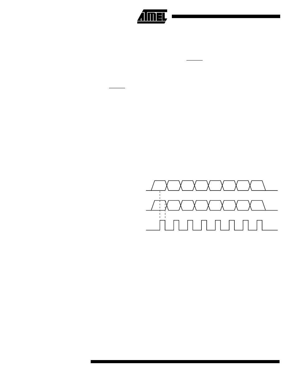
Figure 31. Low-voltage Serial Programming Waveforms
MSB
MSB
LSB
LSB
SERIAL CLOCK INPUT
PB2(SCK)
SERIAL DATA INPUT
PB0(MOSI)
SERIAL DATA OUTPUT
PB1(MISO)