3 sleep mode – Rainbow Electronics ATA6625 User Manual
Page 8
8
4957E–AUTO–10/07
ATA6623/ATA6625
4.3
Sleep Mode
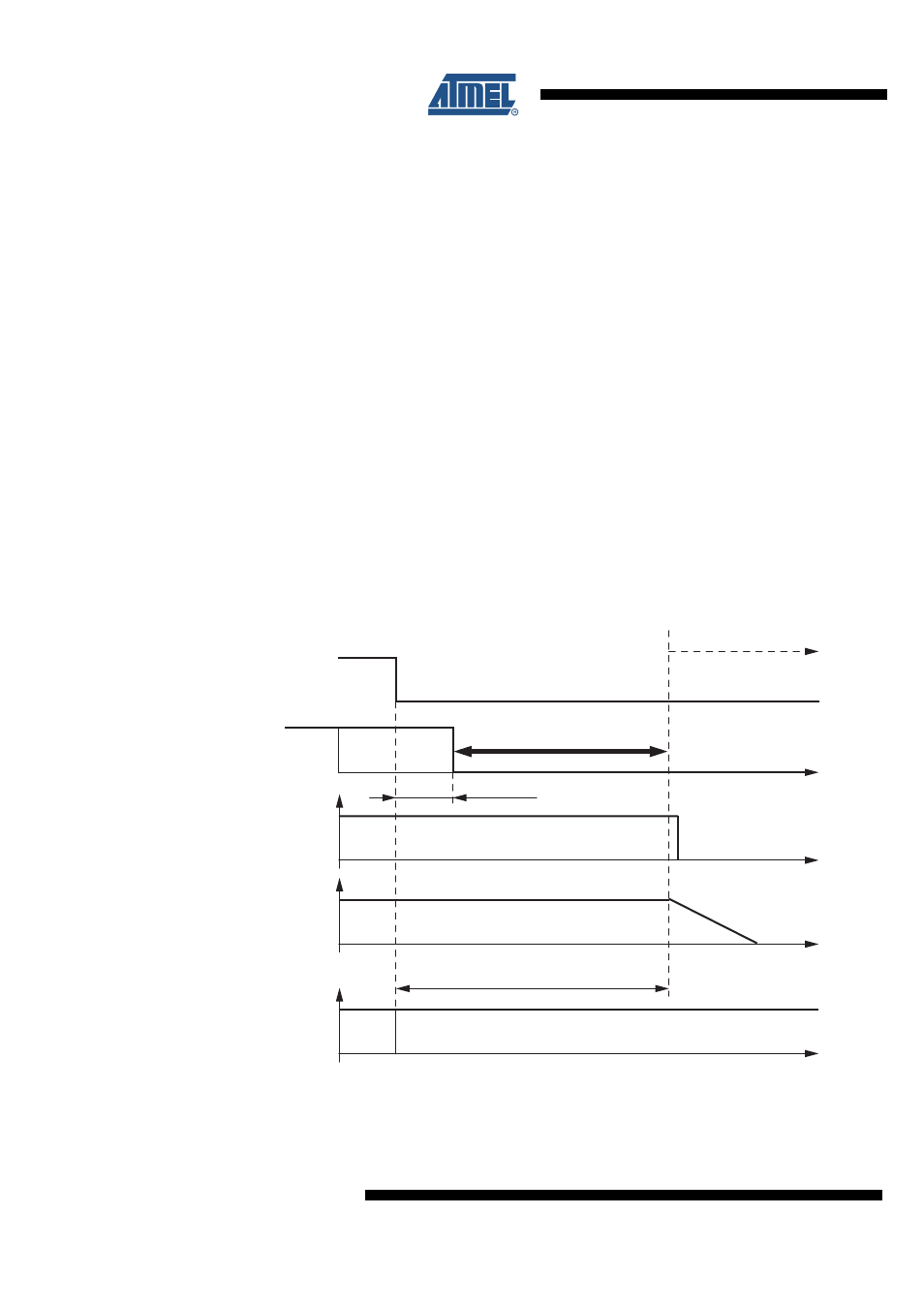
A falling edge at EN while TXD is low switches the IC into Sleep mode. The TXD Signal has to
be logic low during the Mode Select window (
).
In Sleep mode the transmission path is disabled. Supply current from V
Batt
is typically
I
VSsleep
= 10 µA. The V
CC
regulator is switched off; NRES and RXD are low. The internal slave
termination between pin LIN and pin VS is disabled to minimize the power dissipation in case pin
LIN is short-circuited to GND. Only a weak pull-up current (typically 10 µA) between pin LIN and
pin VS is present. The Sleep mode can be activated independently from the current level on pin
LIN.
A voltage less than the LIN Pre-wake detection V
LINL
at pin LIN activates the internal LIN
receiver.
A falling edge at the LIN pin followed by a dominant bus level maintained for a certain time
period (t
bus
) and a following rising edge at pin LIN respectively results in a remote wake-up
request. The device switches from Sleep mode to Fail-safe mode.
The V
CC
regulator is activated, and the internal LIN slave termination resistor is switched on. The
remote wake-up request is indicated by a low level at the RXD pin to interrupt the microcontroller
(
EN high can be used to switch directly from Sleep/Silent to Fail-safe mode. If EN is still high after
VCC ramp up and undervoltage reset time, the IC switches to Normal mode.
Figure 4-4.
Switch to Sleep Mode
Delay time sleep mode
t
d_sleep
= maximum 20 µs
LIN switches directly to recessive mode
t
d
= 3.2 µs
LIN
VCC
NRES
TXD
EN
Sleep Mode
Normal Mode
Mode select window