1 normal mode, 2 silent mode – Rainbow Electronics ATA6625 User Manual
Page 6
6
4957E–AUTO–10/07
ATA6623/ATA6625
4.1
Normal Mode
This is the normal transmitting and Receiving mode of the LIN Interface, in accordance with LIN
specification 2.0. The V
CC
voltage regulator operates with a 3.3V/5V output voltage, with a low
tolerance of ±2% and a maximum output current of 50 mA.
If an undervoltage condition occurs, NRES is switched to low and the IC changes its state to
Fail-safe mode. All features are available.
4.2
Silent Mode
A falling edge at EN while TXD is high switches the IC into Silent mode. The TXD Signal has to
be logic high during the Mode Select window (
). The transmission path is
disabled in Silent mode. The overall supply current from V
Batt
is a combination of the
I
VSsi
= 57 µA plus the V
CC
regulator output current I
VCCs
.
The 3.3V/5V regulator with 2% tolerance can source up to 50 mA. In Silent mode the internal
slave termination between pin LIN and pin VS is disabled to minimize the power dissipation in
case pin LIN is short-circuited to GND. Only a weak pull-up current (typically 10 µA) between pin
LIN and pin VS is present. The Silent mode can be activated independently from the current
level on pin LIN.
If an undervoltage condition occurs, NRES is switched to low and the ATA6623/ATA6625
changes its state to Fail-safe mode.
A voltage less than the LIN Pre-wake detection V
LINL
at pin LIN activates the internal LIN
receiver.
A falling edge at the LIN pin followed by a dominant bus level maintained for a certain time
period (t
bus
) and the following rising edge at pin LIN (see
) results in a
remote wake-up request. The device switches from Silent mode to Fail-safe mode, then the
internal LIN slave termination resistor is switched on. The remote wake-up request is indicated
by a low level at pin RXD to interrupt the microcontroller (
). EN high can be
used to switch directly to Normal mode.
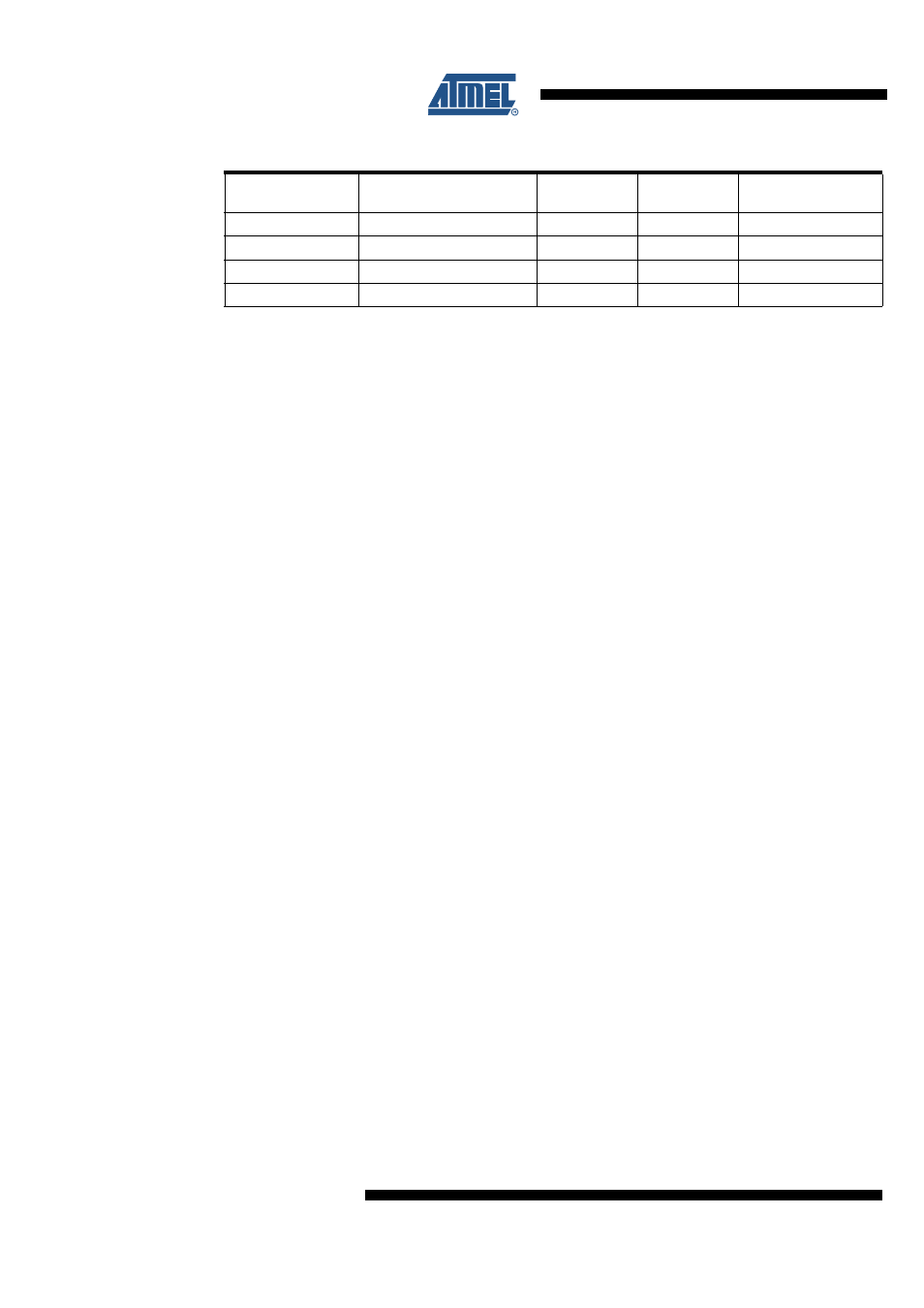
Table 4-1.
Mode of Operation
Mode of
Operation
Transceiver
V
CC
RXD
LIN
Fail safe
OFF
3.3V/5V
High
Recessive
Normal
ON
3.3V/5V
High
TXD depending
Silent
OFF
3.3V/5V
High
Recessive
Sleep
OFF
0V
0V
Recessive