Electrical characteristics (continued) – Rainbow Electronics ATA6625 User Manual
Page 16
16
4957E–AUTO–10/07
ATA6623/ATA6625
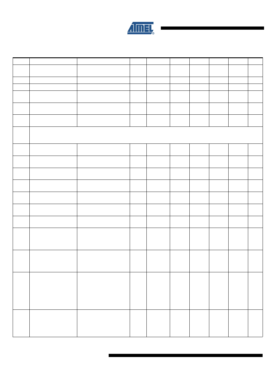
7.7
Load regulation
maximum
5 mA < I
VCC
< 50 mA
VCC
VCC
load
0.5
2
%
A
7.8
Output current limitation VS > 5.5V
VCC
I
VCCs
–200
–160
mA
A
7.9
Load capacity
1
Ω
< ESR < 5
Ω
@ 100 kHz
VCC
C
load
1.8
10
µF
D
7.10
VCC undervoltage
threshold
Referred to VCC
VS > 5.5V
VCC
V
thunN
4.2
4.8
V
A
7.11
Hysteresis of
undervoltage threshold
Referred to VCC
VS > 5.5V
VCC
Vhys
thun
250
mV
A
7.12
Ramp up time VS > 5.5V
to VCC = 5V
C
VCC
= 2.2 µF
I
load
= –5 mA at VCC
VCC
T
VCC
130
300
µs
A
8
LIN Bus Driver: Bus Load Conditions:
Load 1 (Small): 1 nF, 1 k
Ω
; Load 2 (Large): 10 nF, 500
Ω
; R
RXD
= 5 k
Ω
; C
RXD
= 20 pF
10.5, 10.6 and 10.7 Specifies the Timing Parameters for Proper Operation at 20 Kbps
8.1
Driver recessive output
voltage
Load1/Load2
LIN
V
BUSrec
0.9
×
V
S
V
S
V
A
8.2
Driver dominant voltage
V
VS
= 7V
R
load
= 500
Ω
LIN
V
_LoSUP
1.2
V
A
8.3
Driver dominant voltage
V
VS
= 18V
R
load
= 500
Ω
LIN
V
_HiSUP
2
V
A
8.4
Driver dominant voltage
V
VS
= 7V
R
load
= 1000
Ω
LIN
V
_LoSUP_1k
0.6
V
A
8.5
Driver dominant voltage
V
VS
= 18V
R
load
= 1000
Ω
LIN
V
_HiSUP_1k
0.8
V
A
8.6
Pull–up resistor to V
S
The serial diode is
mandatory
LIN
R
LIN
20
30
60
k
Ω
A
8.7
LIN current limitation
V
BUS
= V
Batt_max
LIN
I
BUS_LIM
40
120
200
mA
A
8.8
Input leakage current at
the receiver including
pull-up resistor as
specified
Input Leakage current
Driver off
V
BUS
= 0V
V
Batt
= 12V
LIN
I
BUS_PAS_dom
–1
–0.35
mA
A
8.9
Leakage current LIN
recessive
Driver off
8V < V
Batt
< 18V
8V < V
BUS
< 18V
V
BUS
≥
V
Batt
LIN
I
BUS_PAS_rec
15
20
µA
A
8.10
Leakage current when
control unit disconnected
from ground.
Loss of local ground
must not affect
communication in the
residual network
GND
Device
= V
S
V
Batt
= 12V
0V < V
BUS
< 18V
LIN
I
BUS_NO_gnd
–10
+0.5
+10
µA
A
8.11
Node has to sustain the
current that can flow
under this condition. Bus
must remain operational
under this condition.
V
Batt
disconnected
V
SUP_Device
= GND
0V < V
BUS
< 18V
LIN
I
BUS
5
15
µA
A
8.
Electrical Characteristics (Continued)
5V < V
S
< 27V, –40°C < T
j
< 150°C; unless otherwise specified all values refer to GND pins.
No.
Parameters
Test Conditions
Pin
Symbol
Min.
Typ.
Max.
Unit
Type*
*) Type means: A = 100% tested, B = 100% correlation tested, C = Characterized on samples, D = Design parameter