Rainbow Electronics AT25640 User Manual
Features, Description, Pin configuration
1
Features
•
Serial Peripheral Interface (SPI) Compatible
•
Supports SPI Modes 0 (0,0) and 3 (1,1)
•
Medium-voltage and Standard-voltage Operation
– 5.0 (V
CC
= 4.5V to 5.5V)
– 2.7 (V
CC
= 2.7V to 5.5V)
•
3.0 MHz Clock Rate (5V)
•
32-byte Page Mode
•
Block Write Protection
– Protect 1/4, 1/2, or Entire Array
•
Write Protect (WP) Pin and Write Disable Instructions for
both Hardware and Software Data Protection
•
Self-timed Write Cycle (5 ms Typical)
•
High-reliability
– Endurance: One Million Write Cycles
– Data Retention: 100 Years
•
8-lead PDIP and 8-lead JEDEC SOIC Packages
Description
The AT25080/160/320/640 provides 8192/16384/32768/65536 bits of serial electri-
cal l y-e ra sa bl e pro gramma ble re ad on ly memo r y ( EEPROM ) or ga ni ze d a s
1024/2048/4096/8192 words of 8 bits each. The device is optimized for use in many
automotive applications where low-power and low-voltage operation are essential.
The AT25080/160/320/640 is available in space saving 8-lead PDIP and 8-lead
JEDEC SOIC packages.
The AT25080/160/320/640 is enabled through the Chip Select pin (CS) and accessed
via a 3-wire interface consisting of Serial Data Input (SI), Serial Data Output (SO), and
Serial Clock (SCK). All programming cycles are completely self-timed, and no sepa-
rate ERASE cycle is required before WRITE.
BLOCK WRITE protection is enabled by programming the status register with one of
four blocks of write protection. Separate program enable and program disable instruc-
tions are provided for additional data protection. Hardware data protection is provided
via the WP pin to protect against inadvertent write attempts to the status register. The
HOLD pin may be used to suspend any serial communication without resetting the
serial sequence.
SPI Serial
Automotive
EEPROMs
8K (1024 x 8)
16K (2048 x 8)
32K (4096 x 8)
64K (8192 x 8)
AT25080
AT25160
AT25320
AT25640
3260D–SEEPR–9/03
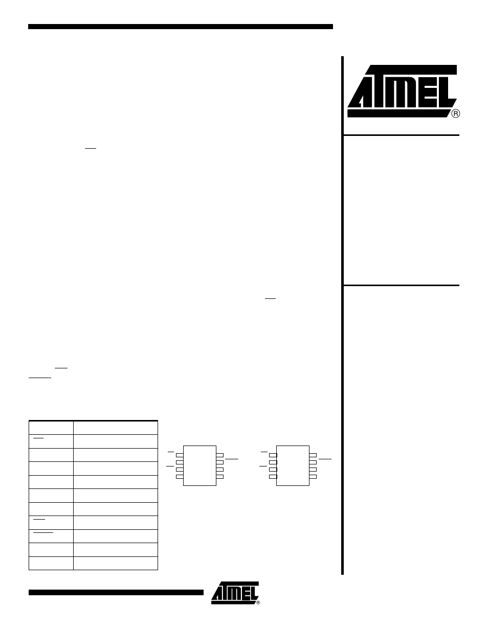
Pin Configuration
Pin Name
Function
CS
Chip Select
SCK
Serial Data Clock
SI
Serial Data Input
SO
Serial Data Output
GND
Ground
VCC
Power Supply
WP
Write Protect
HOLD
Suspends Serial Input
NC
No Connect
DC
Don’t Connect
8-lead PDIP
1
2
3
4
8
7
6
5
CS
SO
WP
GND
VCC
HOLD
SCK
SI
8-lead SOIC
1
2
3
4
8
7
6
5
CS
SO
WP
GND
VCC
HOLD
SCK
SI
Document Outline
- Features
- Description
- Absolute Maximum Ratings*
- Block Diagram
- Pin Capacitance(1)
- DC Characteristics(1)
- AC Characteristics
- Serial Interface Description
- SPI Serial Interface
- Functional Description
- Timing Diagrams
- AT25080 Ordering Information
- AT25160 Ordering Information
- AT25320 Ordering Information
- AT25640 Ordering Information
- Packaging Information
- Pin Configuration