1 functional description – Rainbow Electronics AT77C102B User Manual
Page 10
10
5364A–BIOM–09/05
AT77C102B
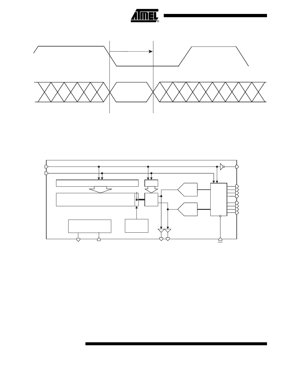
Figure 3-4.
No Data Change
Note:
OE must not change during TNOOE after the PCLK falls. This is to ensure that the output drivers of the data are not driving cur-
rent, so as to reduce the noise level on the power supply.
Figure 3-5.
AT77C102B Block Diagram
3.1
Functional Description
The circuit is divided into two main sections: sensor and data conversion. One particular column
among 280 plus one is selected in the sensor array (1), then each pixel of the selected column
sends its electrical information to the amplifiers (2) [one per line], then two lines at a time are
selected (odd and even) so that two particular pixels send their information to the input of two 4-
bit analog-to-digital converters (3), so two pixels can be read for each clock pulse (4).
PCLK
t
NOOE
OE
2240
8
Latches
Chip
temperature
sensor
Line sel
Odd
Even
8 lines of 280 columns of pixels
4-bit
ADC
ADC
8
1 dummy column
4
4
Amp
Chip temperature
stabilization
ACKN
De0-3
Do0-3
Output
enable
Analog
output
OE
AVE AVO
TPE
TPP
1
8
PCLK
RST
Clock
Reset
Column selection
4-bit