Rainbow Electronics MAX16071 User Manual
Page 30
12-Channel/8-Channel, Flash-Configurable System
Managers with Nonvolatile Fault Registers
MAX16070/MAX16071
30 _____________________________________________________________________________________
Independent Watchdog Timer Operation
When r73h[3] is ‘1’ the watchdog timer operates in
the independent mode. In the independent mode, the
watchdog timer operates as if it were a separate device.
The watchdog timer is activated immediately upon V
CC
exceeding UVLO and once the boot-up sequence is fin-
ished. When RESET is asserted, the watchdog timer and
WDO are not affected.
There will be a startup delay if r76h[6:4] is set to a value
different than ‘000.’ If r76h[6:4] is set to ‘000,’ there will
not be a startup delay. See Table 17 for delay times.
In independent mode, if the Watchdog Reset Output
Enable bit r76h[7] is set to ‘1,’ when the watchdog timer
expires, WDO asserts then RESET asserts. WDO will
then deassert. WDO will be low for approximately 1Fs.
If the Watchdog Reset Output Enable bit (r76h[7]) is set
to ‘0,’ when the WDT expires, WDO asserts but RESET
is not affected.
User-Defined Register
Register r8Ah provides storage space for a user-defined
configuration or firmware version number. Note that this
register controls the contents of the JTAG USERCODE
register bits 7:0. The user-defined register is stored at
r28Ah in the flash memory.
Memory Lock Bits
Register r8Ch contains the lock bits for the configuration
registers, configuration flash, user flash, and fault regis-
ter lock. See Table 18 for details.
SMBus-Compatible Interface
The MAX16070/MAX16071 feature an SMBus-
compatible, 2-wire serial interface consisting of a serial-
data line (SDA) and a serial-clock line (SCL). SDA and
SCL facilitate bidirectional communication between the
MAX16070/MAX16071 and the master device at clock
rates up to 400kHz. Figure 1 shows the 2-wire interface
timing diagram. The MAX16070/MAX16071 are transmit/
receive slave-only devices, relying upon a master device
to generate a clock signal. The master device (typically
a microcontroller) initiates a data transfer on the bus and
generates SCL to permit that transfer.
A master device communicates to the MAX16070/
MAX16071 by transmitting the proper address followed
by a command and/or data words. The slave address
input, A0, is capable of detecting four different states,
allowing multiple identical devices to share the same
serial bus. The slave address is described further in
the Slave Address section. Each transmit sequence is
framed by a START (S) or REPEATED START (SR) con-
dition and a STOP (P) condition. Each word transmitted
over the bus is 8 bits long and is always followed by an
acknowledge pulse. SCL is a logic input, while SDA is
an open-drain input/output. SCL and SDA both require
external pullup resistors to generate the logic-high volt-
age. Use 4.7kI for most applications.
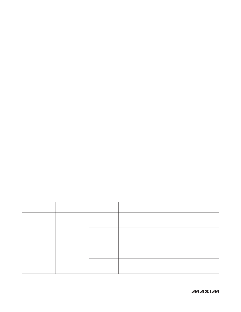
Table
18. Memory Lock Bits
REGISTER
ADDRESS
FLASH ADDRESS
BIT RANGE
DESCRIPTION
8Ch
28Ch
0
Configuration register lock
1 = Locked
0 = Unlocked
1
Flash fault register lock
1 = Locked
0 = Unlocked
2
Flash configuration lock
1 = Locked
0 = Unlocked
3
User flash lock
1 = Locked
0 = Unlocked