Electrical characteristics, Absolute maximum ratings – Rainbow Electronics MAX16071 User Manual
Page 2
12-Channel/8-Channel, Flash-Configurable System
Managers with Nonvolatile Fault Registers
MAX16070/MAX16071
2 ______________________________________________________________________________________
Stresses beyond those listed under “Absolute Maximum Ratings” may cause permanent damage to the device. These are stress ratings only, and functional
operation of the device at these or any other conditions beyond those indicated in the operational sections of the specifications is not implied. Exposure to absolute
maximum rating conditions for extended periods may affect device reliability.
V
CC
, CSP, CSM to GND ........................................-0.3V to +15V
CSP to CSM ..........................................................-0.7V to +0.7V
MON_, GPIO_, SCL, SDA, A0, RESET to GND
(programmed as open-drain outputs) .................-0.3V to +6V
EN, TCK, TMS, TDI to GND ....................................-0.3V to +4V
DBP, ABP to GND ...-0.3V to the lower of +3V and (V
CC
+ 0.3V)
TDO, GPIO_, RESET
(programmed as push-pull outputs) .... -0.3V to (V
DBP
+ 0.3V)
Input/Output Current .........................................................20mA
Continuous Power Dissipation (T
A
= +70NC)
40-Pin TQFN (derate 26.3mW/NC above +70NC) .......2105mW
Operating Temperature Range .......................... -40NC to +85NC
Junction Temperature ....................................................+150NC
Storage Temperature Range ............................ -65NC to +150NC
Lead Temperature (soldering, 10s)
................................+300NC
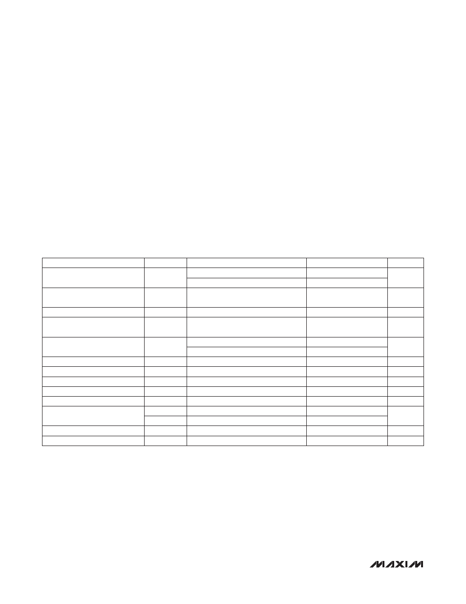
ELECTRICAL CHARACTERISTICS
(V
CC
= 2.8V to 14V, T
A
= -40NC to +85NC, unless otherwise specified. Typical values are at ABP = DBP = V
CC
= 3.3V, T
A
= +25NC.)
(Note 1)
ABSOLUTE MAXIMUM RATINGS
PARAMETER
SYMBOL
CONDITIONS
MIN
TYP
MAX
UNITS
Operating Voltage Range
V
CC
Reset output asserted low
1.2
V
(Note 2)
2.8
14
Undervoltage Lockout (Rising)
V
UVLO
Minimum voltage on V
CC
to ensure the
device is flash configurable
2.7
V
Undervoltage Lockout Hysteresis
V
UVLO_HYS
100
mV
Minimum Flash Operating
Voltage
V
flash
Minimum voltage on V
CC
to ensure flash
erase and write operations
2.7
V
Supply Current
I
CC
No load on output pins
4.5
7
mA
During flash writing cycle
10
14
ABP Regulator Voltage
V
ABP
C
ABP
= 1μF, no load, V
CC
= 5V
2.85
3
3.15
V
DBP Regulator Voltage
V
DBP
C
ABP
= 1μF, no load, V
CC
= 5V
2.8
3
3.1
V
Boot Time
t
BOOT
V
CC
> V
UVLO
200
350
μs
Flash Writing Time
8-byte word
122
ms
Internal Timing Accuracy
(Note 3)
-8
+8
%
EN Input Voltage
V
TH_EN_R
EN voltage rising
1.41
V
V
TH_EN_F
EN voltage falling
1.365
1.39
1.415
EN Input Current
I
EN
-0.5
+0.5
μA
Input Voltage Range
0
5.5
V