Pin description (continued) functional diagram – Rainbow Electronics MAX16068 User Manual
Page 9
_______________________________________________________________________________________ 9
MAX16068
6-Channel, Flash-Configurable System Manager
with Nonvolatile Fault Registers
Pin Description (continued)
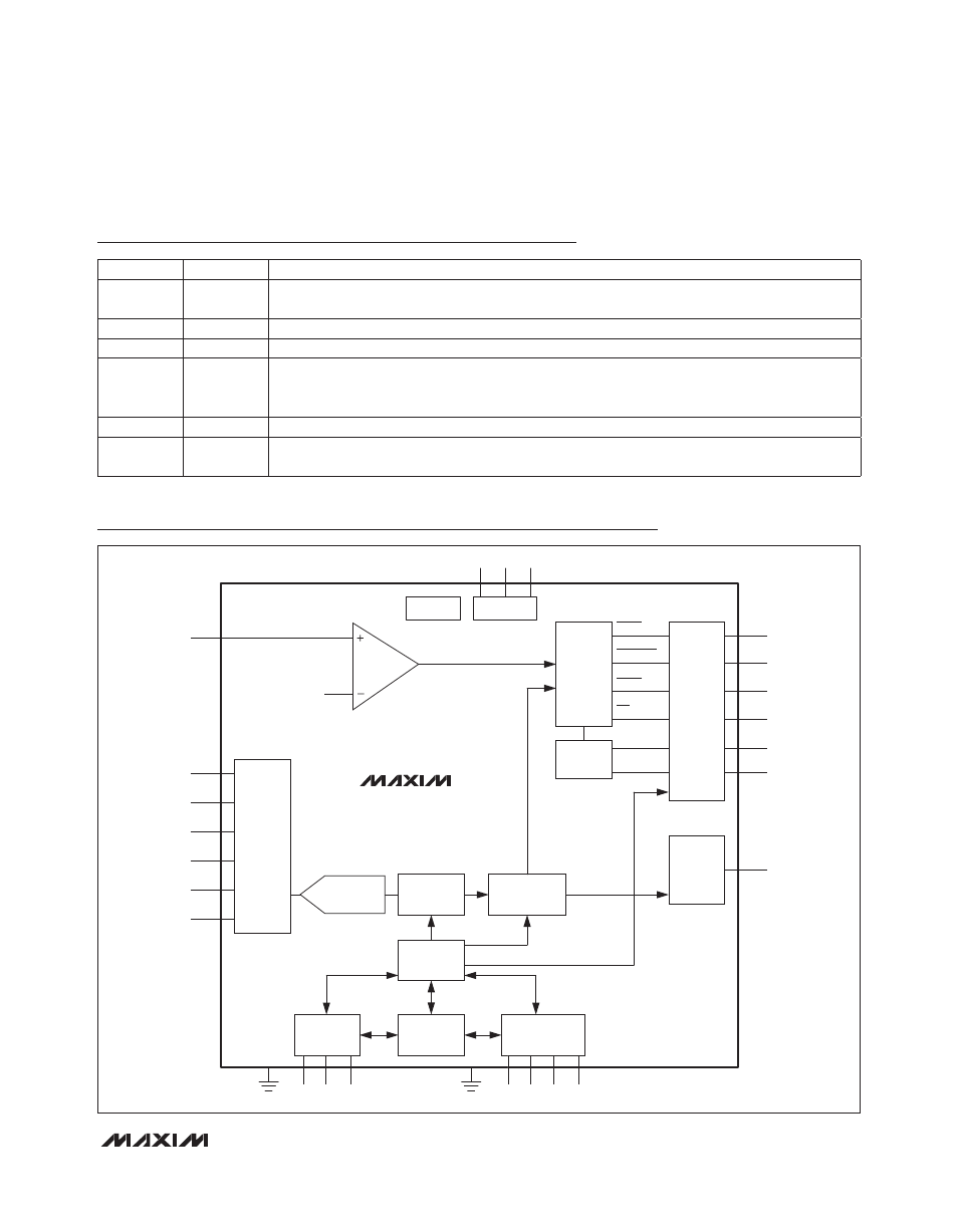
Functional Diagram
GPIO6
WDO
GPIO5
WDI
GPIO4
MR
GPIO3
FAULT
GPIO2
EXTFAULT
GPIO1
ALERT
AO SCL SDA
REF
REG
DECODE
LOGIC
WATCHDOG
TIMER
DIGITAL
COMPARATORS
GPIO
CONTROL
RESET
ABP
V
CC
DBP
RESET
OUTPUT
LOGIC
RAM
REGISTERS
FLASH
REGISTERS
SMBus
INTERFACE
JTAG
INTERFACE
ADC
REGISTERS
10-BIT ADC
(SAR)
EN
V
TH_EN
MON1
MON2
MON3
MON4
MON5
MON6
TDO TDI TCK TMS
GND
GND
MAX16068
VOLTAGE
AND
SCALING
MUX
PIN
NAME
FUNCTION
16
DBP
Digital Bypass. All push-pull outputs are referenced to DBP. Bypass DBP with a 1FF capacitor to
GND.
17
V
CC
Power-Supply Input. Bypass V
CC
to GND with a 10FF ceramic capacitor.
18
ABP
Analog Bypass. Bypass ABP to GND with a 1FF ceramic capacitor.
20–25
MON1–
MON6
Monitor Voltage Inputs. Set the monitor voltage range through the configuration registers.
Measured values are written to the ADC registers and can be read back through the SMBus or
JTAG interface.
26
RESET
Configurable Reset Output
—
EP
Exposed Pad. Internally connected to GND. Connect to ground, but do not use EP as the main
ground connection.