Rainbow Electronics MAX16068 User Manual
Page 23
______________________________________________________________________________________ 23
MAX16068
6-Channel, Flash-Configurable System Manager
with Nonvolatile Fault Registers
The watchdog can be configured to control the RESET
output as well as the WDO output. RESET asserts for
the reset timeout, t
RP
, when the watchdog timer expires
and the Watchdog Reset Output Enable bit (r76h[7]) is
set to ‘1’. When RESET is asserted, the watchdog timer
is cleared and WDO is deasserted, therefore, WDO
pulses low for a short time (approximately 1Fs) when
the watchdog timer expires. RESET is not affected by
the watchdog timer when the Watchdog Reset Output
Enable bit (r76h[7]) is set to ‘0’. If a RESET is asserted
by the watchdog timeout, the WDRESET bit is set to ‘1’. A
connected processor can check this bit to see the reset
was due to a watchdog timeout.
See Table 16 for more information on configuring watch-
dog functionality.
Independent Watchdog Timer Operation
When r73h[3] is ‘1,’ the watchdog timer operates in
the independent mode. In the independent mode, the
watchdog timer operates as if it were a separate device.
The watchdog timer is activated immediately upon V
CC
exceeding UVLO and once the boot-up sequence is
finished. When RESET is asserted by EN being low, the
watchdog timer and WDO are not affected.
There is a startup delay if r76h[6:4] is set to a value dif-
ferent than ‘000’. If r76h[6:4] is set to ‘000’, there is not
a startup delay. See Table 16 for delay times.
In independent mode, if the Watchdog Reset Output
Enable bit r76h[7] is set to ‘1,’ when the watchdog timer
expires, WDO asserts then RESET asserts. WDO then
deasserts. WDO is low for approximately 1Fs. If the
Watchdog Reset Output Enable bit (r76h[7]) is set to
‘0,’ when the watchdog timer expires, WDO asserts but
RESET is not affected.
User-Defined Register
Register r8Ah provides storage space for a user-defined
configuration or firmware version number. Note that this
register controls the contents of the JTAG USERCODE
register bits 7-0. The user-defined register is stored at
r28Ah in the flash memory.
Memory Lock Bits
Register r8Ch contains the lock bits for the configuration
registers, configuration flash, user flash, and fault regis-
ter lock. See Table 17 for details.
SMBus-Compatible Interface
The MAX16068 features an SMBus-compatible, 2-wire
serial interface consisting of a serial-data line (SDA)
and a serial-clock line (SCL). SDA and SCL facilitate
bidirectional communication between the MAX16068
and the master device at clock rates up to 400kHz.
Figure 1 shows the 2-wire interface timing diagram. The
MAX16068 is a transmit/receive, slave-only device, rely-
ing upon a master device to generate a clock signal.
The master device (typically a microcontroller) initiates
a data transfer on the bus and generates SCL to permit
that transfer.
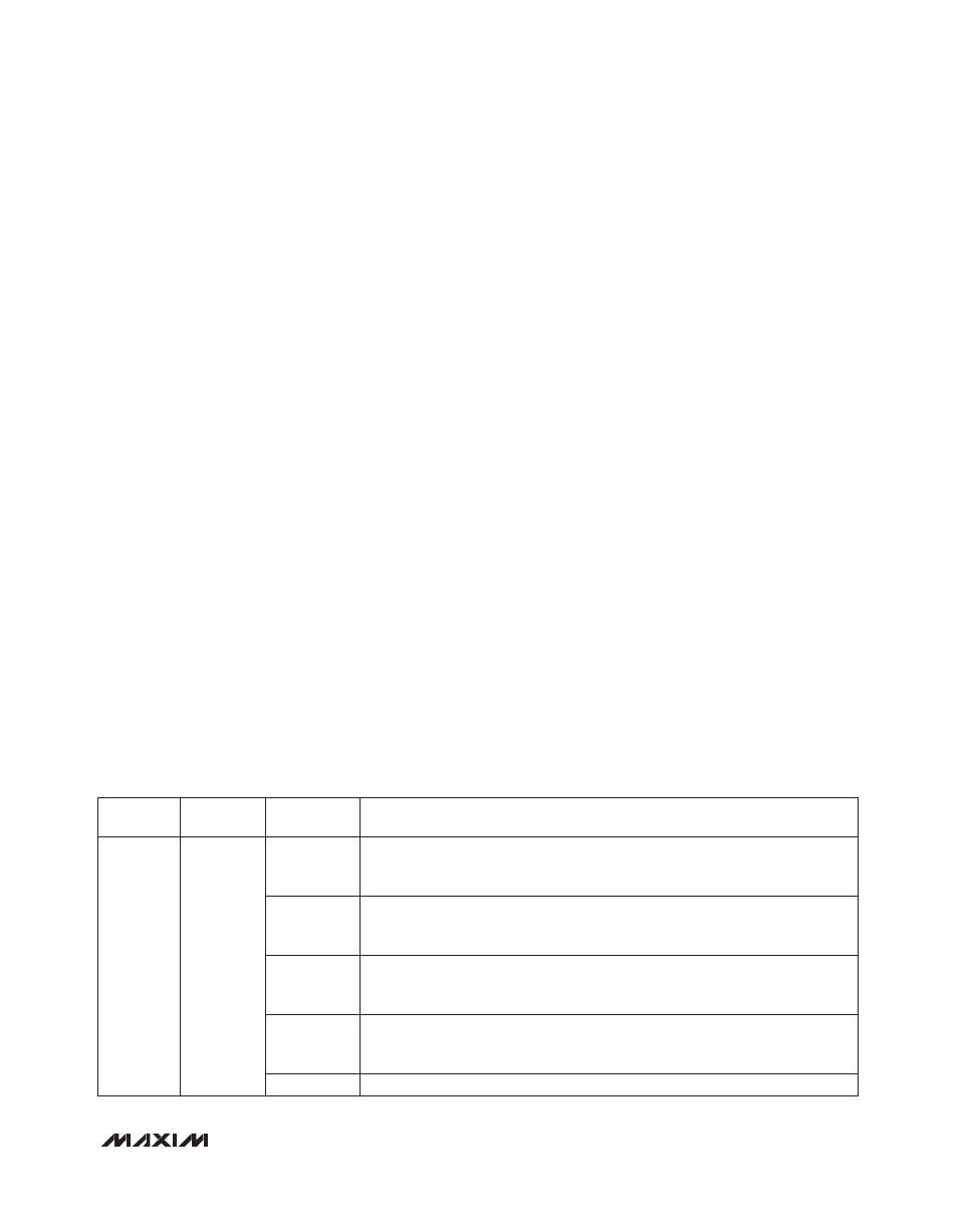
Table 17. Memory Lock Bits
REGISTER
ADDRESS
FLASH
ADDRESS
BIT RANGE
DESCRIPTION
8Ch
28Ch
[0]
Configuration Register Lock
1 = Locked
0 = Unlocked
[1]
Flash Fault Register Lock
1 = Locked
0 = Unlocked
[2]
Flash Configuration Lock
1 = Locked
0 = Unlocked
[3]
User Flash Lock
1 = Locked
0 = Unlocked
[7.4]
Not used