Pin description pin configuration – Rainbow Electronics MAX16068 User Manual
Page 8
8 ______________________________________________________________________________________
MAX16068
6-Channel, Flash-Configurable System Manager
with Nonvolatile Fault Registers
Pin Description
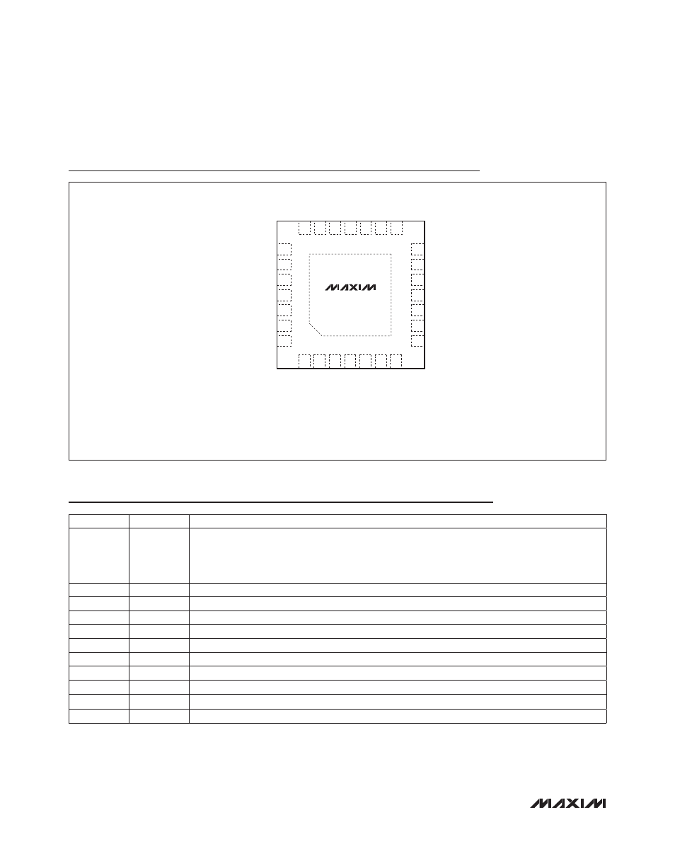
Pin Configuration
MAX16068
THIN QFN
(5mm x 5mm)
TOP VIEW
26
27
25
24
10
9
11
12
1
2
4
5
6
7
EP*
20
21
19
17
16 15
3
18
28
8
+
23
13
22
14
GPIO4
GPIO6
GND
AO
SCL
GPIO3
MON1
ABP
V
CC
MON2
DBP
EN
MON5
MON6
RESET
N.C.
TMS
TCK
TDI
GPIO5
GND
GPIO1
TDO
GPIO2
SDA
MON4
N.C.
MON3
*CONNECT EXPOSED PAD TO GND.
PIN
NAME
FUNCTION
1–4, 27, 28
GPIO3–
GPIO6,
GPIO1,
GPIO2
General-Purpose Inputs/Outputs. Each GPIO_ can be configured to act as an input, a push-pull
output, an open-drain output, or a special function.
5, 19
GND
Ground. Connect all GNDs together.
6
A0
Four-State SMBus Address. Address is sampled upon POR.
7
SCL
SMBus Serial-Clock Input
8
SDA
SMBus Serial-Data Open-Drain Input/Output
9
TDO
JTAG Test Data Output
10
TDI
JTAG Test Data Input
11
TCK
JTAG Test Clock
12
TMS
JTAG Test Mode Select
13, 14
N.C.
No Connection. Not internally connected.
15
EN
Analog Enable Input. All outputs deassert when V
EN
is below the enable threshold.