Electrical characteristics, Absolute maximum ratings – Rainbow Electronics MAX16068 User Manual
Page 2
2 ______________________________________________________________________________________
MAX16068
6-Channel, Flash-Configurable System Manager
with Nonvolatile Fault Registers
Stresses beyond those listed under “Absolute Maximum Ratings” may cause permanent damage to the device. These are stress ratings only, and functional
operation of the device at these or any other conditions beyond those indicated in the operational sections of the specifications is not implied. Exposure to absolute
maximum rating conditions for extended periods may affect device reliability.
V
CC
to GND ...............……………………………….-0.3V to +15V
MON_, SCL, SDA, A0 to GND ................................-0.3V to +6V
EN, TCK, TMS, TDI to GND ....................................-0.3V to +4V
TDO to GND ............................................-0.3V to (V
DBP
+ 0.3V)
RESET, GPIO_
(configured as open-drain) to GND. ....................-0.3V to +6V
RESET, GPIO_ (configured as push-pull)
to GND .................................................-0.3V to (V
DBP
+ 0.3V)
DBP, ABP to GND .......................................-0.3V to minimum of
(4V and (V
CC
+ 0.3V))
Continuous Current (all pins) .......................................... Q20mA
Continuous Power Dissipation (T
A
= +70NC)
28-Pin TQFN (derate 34.5mW/NC above +70NC) ..... 2759mW*
Thermal Resistance (Note 1)
B
JA
................................................................................29NC/W
B
JC
........................…………………………….………… 2NC/W
Operating Temperature Range .......................... -40NC to +85NC
Junction Temperature .....................................................+150NC
Storage Temperature Range ............................ -65NC to +150NC
Lead Temperature (soldering, 10s) ................................+300NC
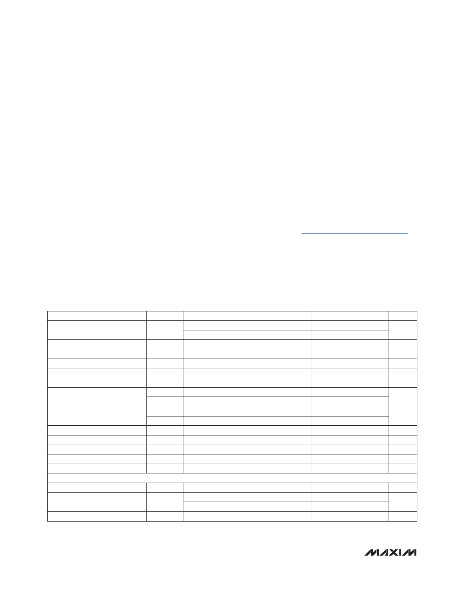
ELECTRICAL CHARACTERISTICS
(V
CC
= 2.8V to 14V, T
A
= T
J
= -40NC to +85NC, unless otherwise specified. Typical values are at V
ABP
= V
DBP
= V
CC
= 3.3V,
T
A
= +25NC.) (Note 2)
ABSOLUTE MAXIMUM RATINGS
*As per JEDEC 51 Standard, Multilayer Board (PCB).
Note 1: Package thermal resistances were obtained using the method described in JEDEC specification JESD51-7, using a four-
layer board. For detailed information on package thermal considerations, refer
.
PARAMETER
SYMBOL
CONDITIONS
MIN
TYP
MAX
UNITS
Operating Voltage Range
V
CC
RESET output asserted low
1.2
V
2.8
14
Undervoltage Lockout
V
UVLO
Minimum voltage on V
CC
to ensure the
device is flash configurable
2.7
V
Undervoltage Lockout Hysteresis
UVLO
HYS
55
mV
Minimum Flash Operating Voltage
V
FLASH
Minimum voltage on V
CC
to ensure flash
erase and write operations
2.7
V
Supply Current
I
CC1
No load on any output
2.8
4
mA
I
CC2
No load on any output, during flash writing
cycle
7.7
14
V
CC
= V
ABP
= V
DBP
= 3.6V (Note 3)
5
DBP Regulator Voltage
V
DBP
V
CC
= 5V, C
DBP
= 1FF, no load
2.8
3
3.2
V
ABP Regulator Voltage
V
ABP
V
CC
= 5V, C
ABP
= 1FF, no load
2.85
3
3.15
V
Boot Time
t
BOOT
V
CC
> V
UVLO
100
200
F
s
Flash Writing Time
8-byte word
122
ms
Internal Timing Accuracy
(Note 4)
-10
+10
%
ADC
Resolution
10
Bits
Gain Error
ADC
GAIN
T
A
= +25NC
0.35
%
T
A
= -40NC to +85NC
0.75
Offset Error
ADC
OFF
1.5
LSB