Electrical characteristics (continued) – Rainbow Electronics MAX16068 User Manual
Page 4
4 ______________________________________________________________________________________
MAX16068
6-Channel, Flash-Configurable System Manager
with Nonvolatile Fault Registers
ELECTRICAL CHARACTERISTICS (continued)
(V
CC
= 2.8V to 14V, T
A
= T
J
= -40NC to +85NC, unless otherwise specified. Typical values are at V
ABP
= V
DBP
= V
CC
= 3.3V,
T
A
= +25NC.) (Note 2)
Note 2: Specifications are guaranteed for the stated global conditions, unless otherwise noted. 100% production tested at T
A
=
+25NC and T
A
= +85NC. Specifications at T
A
= -40NC are guaranteed by design.
Note 3: For V
CC
of 3.6V or lower, connect V
CC
, DBP, and ABP together. For higher supply applications, connect only V
CC
to the
supply rail.
Note 4: Applies to RESET (except for a reset timeout period of 25Fs), fault, autoretry, sequence delays, and watchdog timeout.
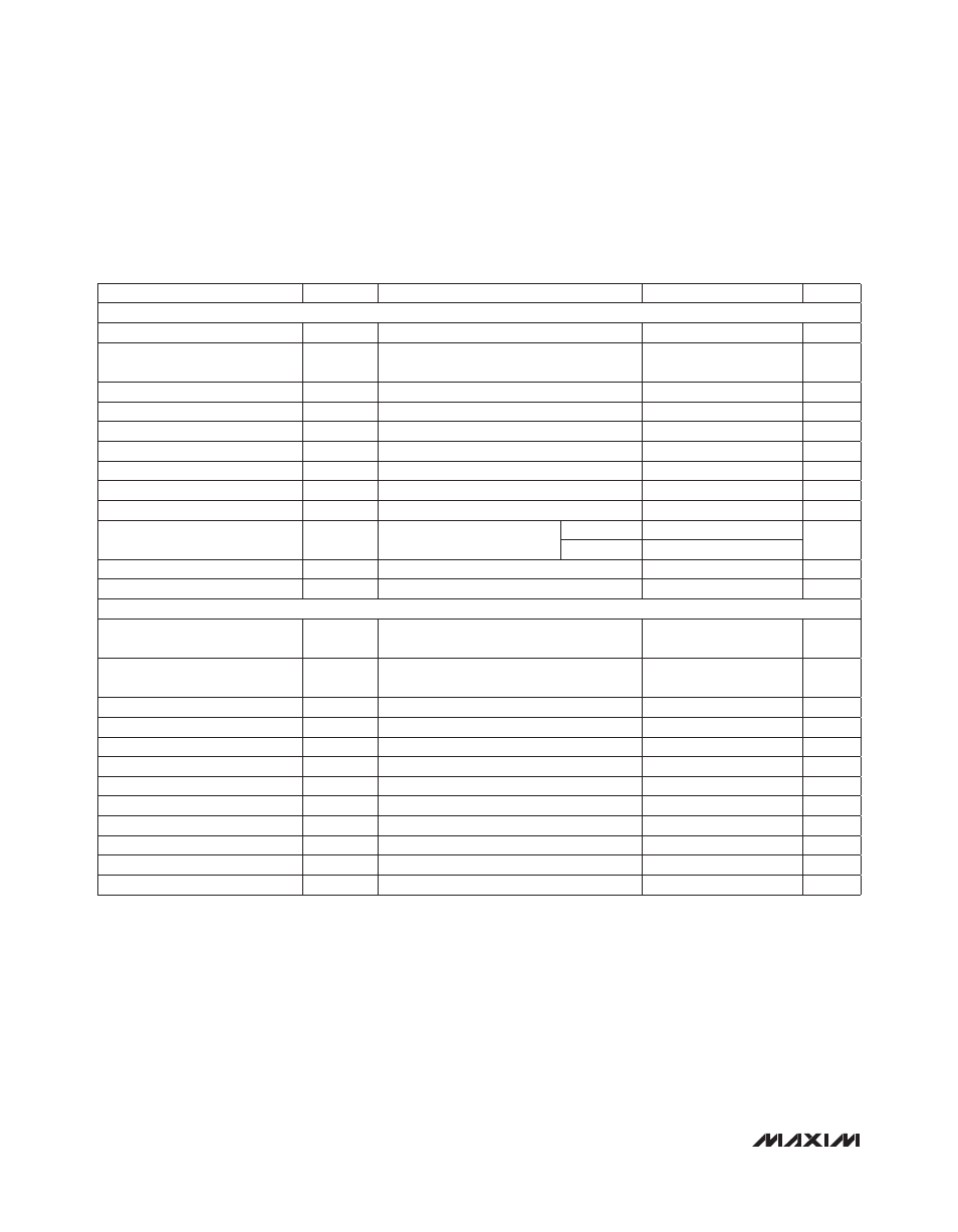
PARAMETER
SYMBOL
CONDITIONS
MIN
TYP
MAX
UNITS
SMBus TIMING
Serial Clock Frequency
f
SCL
400
kHz
Bus Free Time Between STOP
and START Condition
t
BUF
1.3
F
s
START Condition Setup Time
t
SU:STA
0.6
F
s
START Condition Hold Time
t
HD:STA
0.6
F
s
STOP Condition Setup Time
t
SU:STO
0.6
F
s
Clock Low Period
t
LOW
1.3
F
s
Clock High Period
t
HIGH
0.6
F
s
Data Setup Time
t
SU:DAT
100
ns
Output Fall Time
t
OF
10pF P C
BUS
P
400pF
250
ns
Data Hold Time
t
HD:DAT
From 50% SCL falling to SDA
change
Receive
0.15
F
s
Transmit
0.3
0.9
Pulse Width of Spike Suppressed
t
SP
250
ns
SMBus Timeout
t
TIMEOUT
SMBCLK time low for reset
22
35
ms
JTAG INTERFACE
TDI, TMS, TCK Logic-Low Input
Voltage
V
IL
Input voltage falling
0.8
V
TDI, TMS, TCK Logic-High Input
Voltage
V
IH
Input voltage rising
2.0
V
TDO Logic-Output Low Voltage
V
OL_TDO
I
SINK
= 3mA
0.4
V
TDO Logic-Output High Voltage
V
OH_TDO
I
SOURCE
= 200FA
2.4
V
TDI, TMS Pullup Resistors
R
JPU
Pullup to DBP
30
50
65
kI
I/O Capacitance
C
I/O
5
pF
TCK Clock Period
t
1
1000
ns
TCK High/Low Time
t
2,
t
3
50
500
ns
TCK to TMS, TDI Setup Time
t
4
15
ns
TCK to TMS, TDI Hold Time
t
5
15
ns
TCK to TDO Delay
t
6
500
ns
TCK to TDO High-Z Delay
t
7
500
ns