Rainbow Electronics MAX16068 User Manual
Page 34
34 _____________________________________________________________________________________
MAX16068
6-Channel, Flash-Configurable System Manager
with Nonvolatile Fault Registers
USERCODE: When the USERCODE instruction latches
into the parallel instruction register, the user-code data
register is selected. The device user-code loads into the
user-code data register on the rising edge of TCK fol-
lowing entry into the capture-DR state. Shift-DR can be
used to shift the user-code out serially through TDO. See
Table 24. This instruction can be used to help identify
multiple MAX16068 devices connected in a JTAG chain.
LOAD ADDRESS: This is an extension to the standard
IEEE 1149.1 instruction set to support access to the
memory in the MAX16068. When the LOAD ADDRESS
instruction latches into the instruction register, TDI con-
nects to TDO through the 8-bit memory address test
data register during the shift-DR state.
READ DATA: This is an extension to the standard
IEEE 1149.1 instruction set to support access to the
memory in the MAX16068. When the READ instruction
latches into the instruction register, TDI connects to TDO
through the 8-bit memory read test data register during
the shift-DR state.
WRITE DATA: This is an extension to the standard
IEEE 1149.1 instruction set to support access to the
memory in the MAX16068. When the WRITE instruction
latches into the instruction register, TDI connects to TDO
through the 8-bit memory write test data register during
the shift-DR state.
REBOOT: This is an extension to the standard IEEE
1149.1 instruction set to initiate a software-controlled
reset to the MAX16068. When the REBOOT instruc-
tion latches into the instruction register, the MAX16068
resets and immediately begins the boot-up sequence.
SAVE: This is an extension to the standard IEEE 1149.1
instruction set that triggers a fault log. The current ADC
conversion results along with fault information are saved
to flash depending on the configuration of the Critical
Fault Log Control register (r6Dh).
SETFLSHADD: This is an extension to the standard
IEEE 1149.1 instruction set that allows access to the
flash page. Flash registers include ADC conversion
results, DACOUT enables, and GPIO input/output data.
Use this page to access registers 200h–2FFh.
RSTFLSHADD: This is an extension to the standard
IEEE 1149.1 instruction set. Use RSTFLSHADD to return
to the default page and disable access to the flash page.
SETUSRFLSH: This is an extension to the standard
IEEE 1149.1 instruction set that allows access to the user
flash page. When on the configuration flash page, send
the SETUSRFLSH command, all addresses are recog-
nized as flash addresses only. Use this page to access
registers 300h–3FFh.
RSTUSRFLSH: This is an extension to the standard
IEEE 1149.1 instruction set. Use RSTUSRFLSH to return
to the configuration flash page and disable access to
the user flash.
Restrictions When Writing to Flash
Flash must be written to 8 bytes at a time. The initial
address must be aligned to 8-byte boundaries—the 3
LSBs of the initial address must be ‘000’. Write the 8
bytes using eight successive Write Data commands. A
write operation requires 122ms for each 8-byte block.
After programming a block, check r20h[1] (see Table
25) to make sure the write operation is complete before
attempting to write the next block.
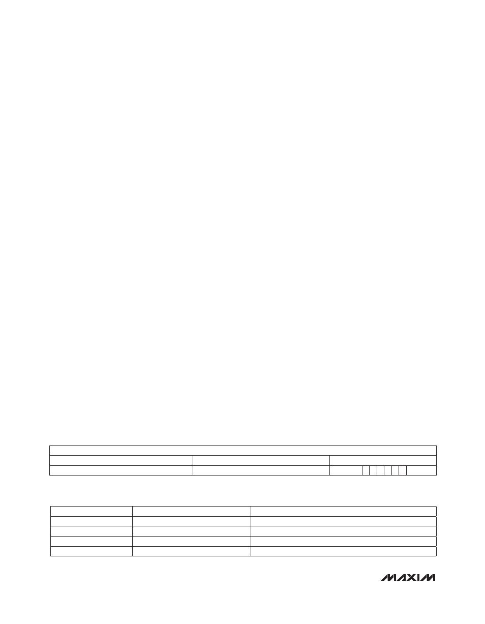
Table 23. 32-Bit User-Code Data
Table 24. Maximum Write Time
MSB
LSB
DON’T CARE
SMBUS SLAVE ID
USER ID (r8A[7:0])
00000000000000000
See Table 18
r6Dh[1:0] VALUE
DESCRIPTION
MAXIMUM WRITE TIME (ms)
00
Save flags and ADC readings
153
01
Save flags
102
10
Save ADC readings
153
11
Do not save anything
—