Detailed description, Pin description – Rainbow Electronics MAX19996A User Manual
Page 30
Detailed Description
When used as a high-side LO injection mixer in the
2300MHz to 2900MHz RF band, the MAX19996A pro-
vides 8.7dB of conversion gain and +24.5dBm of IIP3
with a typical noise figure of 9.8dB. The integrated
baluns and matching circuitry allow for 50
Ω single-
ended interfaces to the RF and the LO ports. The inte-
grated LO buffer provides a high drive level to the
mixer core, reducing the LO drive required at the
MAX19996A’s input to a -3dBm to +3dBm range. The IF
port incorporates a differential output, which is ideal for
providing enhanced 2LO-2RF performance.
Specifications are guaranteed over broad frequency
ranges to allow for use in WCS, LTE, WiMAX, and
MMDS base stations. The MAX19996A is specified to
operate over an RF input range of 2000MHz to
3900MHz, an LO range of 2100MHz to 4000MHz, and
an IF range of 50MHz to 500MHz. The external IF com-
ponents set the lower frequency range (see the
Typical
Operating Characteristics
for details). Operation
beyond these ranges is possible (see the
Typical
Operating Characteristics
for additional information).
RF Input and Balun
The MAX19996A RF input provides a 50
Ω match when
combined with a series DC-blocking capacitor. This
DC-blocking capacitor is required as the input is inter-
nally DC shorted to ground through the on-chip balun.
When using an 8.2pF DC-blocking capacitor, the RF
port input return loss is typically 14dB over the RF fre-
quency range of 2300MHz to 2900MHz. A return loss of
15dB over the 3000MHz to 3900MHz range can be
achieved by changing the DC-blocking capacitor to
1.5pF.
LO Inputs, Buffer, and Balun
With a broadband LO drive circuit spanning 2100MHz
to 4000MHz, the MAX19996A can be used in either
low-side or high-side LO injection architectures for vir-
tually all 2.5GHz and 3.5GHz applications. The LO
input is internally matched to 50
Ω, requiring only a 2pF
DC-blocking capacitor. A two-stage internal LO buffer
allows for a -3dBm to +3dBm LO input power range.
The on-chip low-loss balun, along with an LO buffer,
drives the double-balanced mixer. All interfacing and
matching components from the LO inputs to the IF out-
puts are integrated on-chip.
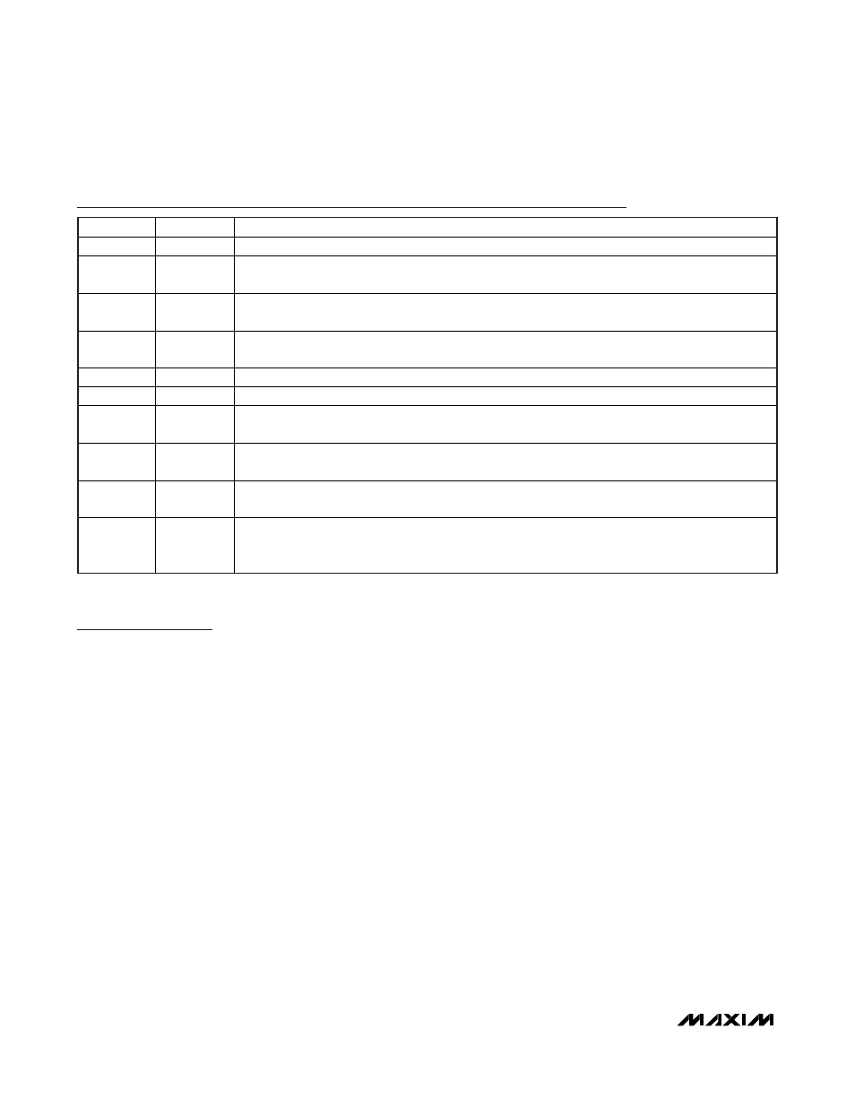
Pin Description
PIN
NAME
FUNCTION
1, 6, 8, 14
V
CC
Power Supply. Bypass to GND with 0.01µF capacitors as close as possible to the pin.
2
RF
Single-Ended 50
Ω RF Input. Internally matched and DC shorted to GND through a balun. Requires an
input DC-blocking capacitor.
3, 4, 5, 10,
12, 13, 17
GND
Ground. Internally connected to the exposed pad. Connect all ground pins and the exposed pad (EP)
together.
7
LOBIAS
LO Amplifier Bias Control. Output bias resistor for the LO buffer. Connect a 604
Ω 1% (230mA bias
condition) from LOBIAS to ground.
9, 15
N.C.
Not internally connected. Pins can be grounded.
11
LO
Local O sci l l ator Inp ut. Thi s i np ut i s i nter nal l y m atched to 50
Ω . Req ui r es an i np ut D C - b l ocki ng cap aci tor .
16
LEXT
E xter nal Ind uctor C onnecti on. C onnect an i nd uctor fr om thi s p i n to g r ound to i ncr ease the RF- to- IF and
LO- to- IF i sol ati on ( see the Typ i cal Op er ati ng C har acter i sti cs for typ i cal p er for m ance vs. i nd uctor val ue) .
18, 19
IF-, IF+
Mixer Differential IF Output. Connect pullup inductors from each of these pins to V
CC
(see the Typical
Application Circuit).
20
IFBIAS
IF Amplifier Bias Control. IF bias resistor connection for the IF amplifier. Connect a 698
Ω 1% (230mA
bias condition) from IFBIAS to GND.
—
EP
Exposed Pad. Internally connected to GND. Solder this exposed pad to a PCB pad that uses multiple
ground vias to provide heat transfer out of the device into the PCB ground planes. These multiple via
grounds are also required to achieve the noted RF performance.
30
______________________________________________________________________________________
SiGe, High-Linearity, 2000MHz to 3900MHz
Downconversion Mixer with LO Buffer
MAX19996A