Preliminary w24l11, Write cycle 1, Write cycle 2 – Rainbow Electronics W24L11 User Manual
Page 6: Oe = v, Fixed)

Preliminary W24L11
- 6 -
Timing Waveforms, continued
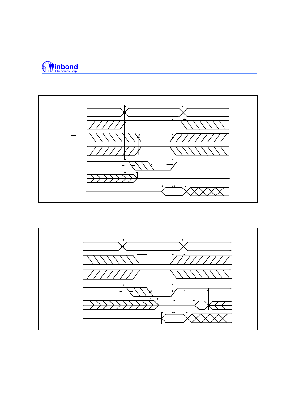
Write Cycle 1
Address
OE
T
WC
T
WR
WE
D
OUT
D
IN
T
WP
T
AS
T
OHZ
(1, 4)
T
DW
T
DH
T
AW
CS1
T
CW
CS2
Write Cycle 2
(OE = V
IL
Fixed)
WE
D
OUT
D
IN
T
AS
T
DH
T
WP
T
WHZ
DW
T
(2)
(3)
T
OW
T
OH
AW
T
(1, 4)
T
CW
T
WR
Address
T
WC
CS1
CS2
Notes:
1. During this period, I/O pins are in the output state, so input signals of opposite phase to the outputs should not be applied.
2. The data output from D
OUT
are the same as the data written to D
IN
during the write cycle.
3. D
OUT
provides the read data for the next address.
4. Transition is measured
±
500 mV from steady state with C
L
= 5 pF. This parameter is guaranteed but not 100% tested.
See also other documents in the category Rainbow Electronics Storage:
- W27E010 (14 pages)
- W27L520 (16 pages)
- W29EE512 (21 pages)
- W27E512 (16 pages)
- W24100 (11 pages)
- W27E040 (15 pages)
- W25Q32 (60 pages)
- W49L102 (21 pages)
- W29C040 (20 pages)
- W29EE011 (20 pages)
- W49F020 (21 pages)
- W2465 (10 pages)
- W24256 (10 pages)
- W982516CH (43 pages)
- MAX16014 (12 pages)
- W24512A (10 pages)
- W27E020 (14 pages)
- W29C020C (21 pages)
- W25X64 (47 pages)
- W24257 (11 pages)
- W24L257 (10 pages)
- W9864G2GH (48 pages)
- W27L010 (14 pages)
- W27E520 (16 pages)
- W27LE520 (16 pages)
- W9825G6CH (43 pages)
- W49F002U (23 pages)
- W9864G6GB (47 pages)
- AT45DB011B (32 pages)
- AT45DB642 (37 pages)
- AT45DB642 (71 pages)
- AT45DB161D (51 pages)
- AT27LV040A (12 pages)
- AT29LV010A (15 pages)
- HT24LC08 (11 pages)
- AT29C257 (12 pages)
- AT45DB161B (32 pages)
- AT27C1024 (12 pages)
- AT28BV256 (12 pages)
- AT28C040 (12 pages)
- DS1258Y_AB (9 pages)
- AT28BV64B (12 pages)
- AT27C512R (12 pages)
- DS1220AB_AD (9 pages)
