Rainbow Electronics MAX6959 User Manual
Page 7
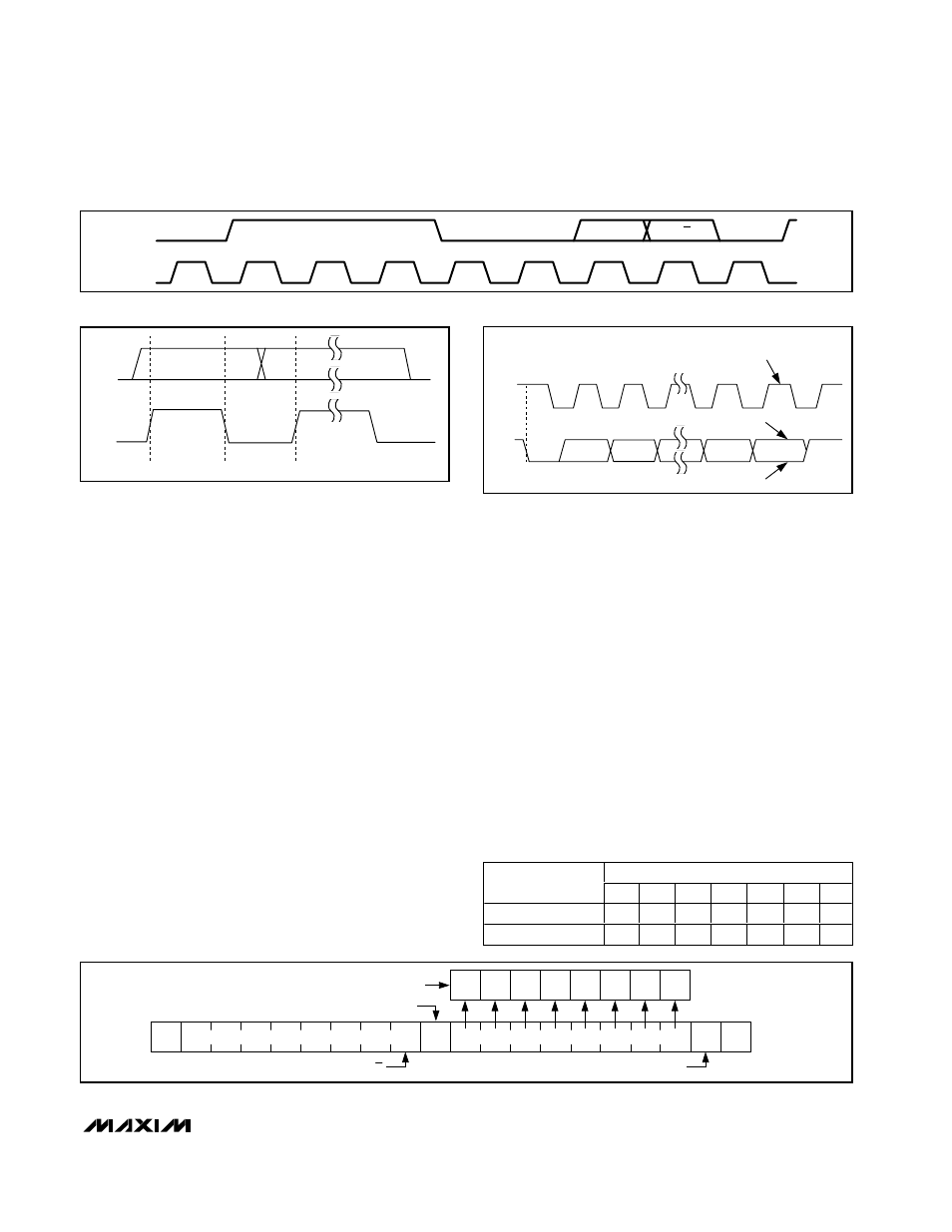
Bit Transfer
One data bit is transferred during each clock pulse.
The data on the SDA line must remain stable while SCL
is high (Figure 4).
Acknowledge
The acknowledge bit is a clocked 9th bit that the recipi-
ent uses to handshake receipt of each byte of data
(Figure 5). Thus, each byte transferred effectively
requires 9 bits. The master generates the 9th clock
pulse, and the recipient pulls down SDA during the
acknowledge clock pulse, such that the SDA line is sta-
ble low during the high period of the clock pulse. When
the master is transmitting to the MAX6958/MAX6959,
the MAX6958/MAX6959 generate the acknowledge bit
because the MAX6958/MAX6959 are the recipients.
When the MAX6958/MAX6959 are transmitting to the
master, the master generates the acknowledge bit
because the master is the recipient.
Slave Address
The MAX6958/MAX6959 have a 7-bit-long slave
address (Figure 3). The eighth bit following the 7-bit
slave address is the R/W bit. Set the R/W bit low for a
write command and high for a read command.
The MAX6958/MAX6959 are available in one of two
possible slave addresses (see Table 2 and Ordering
Information). The first 6 bits (MSBs) of the MAX6958/
MAX6959 slave address are always 011100. Slave
address bit A0 is internally hardwired to either GND in
the MAX695_A_, or V+ in the MAX695_B_. A maximum
of two MAX6958/MAX6959 devices can share a bus.
Message Format for Writing
A write to the MAX6958/MAX6959 comprises the trans-
mission of the MAX6958/MAX6959s’ slave address with
the R/W bit set to zero, followed by at least 1 byte of
information. The first byte of information is the com-
mand byte, which determines the register that stores
the next byte written to the MAX6958/MAX6959. If a
STOP condition is detected after the command byte is
received, the MAX6958/MAX6959 take no further action
(Figure 6) beyond storing the command byte.
MAX6958/MAX6959
2-Wire Interfaced, 3V to 5.5V, 4-Digit,
9-Segment LED Display Drivers with Keyscan
_______________________________________________________________________________________
7
SDA
SCL
0
1
A0
MSB
LSB
R/W
ACK
1
1
0
0
Figure 3. Slave Address
SDA
DATA STABLE,
DATA VALID
CHANGE OF
DATA ALLOWED
SCL
Figure 4. Bit Transfer
1
SCL
START
CONDITION
SDA
2
8
9
CLOCK PULSE FOR
ACKNOWLEDGMENT
ACKNOWLEDGE
NOT ACKNOWLEDGE
Figure 5. Acknowledge
MAX6958/MAX6959 DEVICE ADDRESS
SLAVE ADDRESS
BIT A0
A6
A5
A4
A3
A2
A1
A0
MAX695_A_
0
1
1
1
0
0
0
MAX695_B_
0
1
1
1
0
0
1
Table 2. MAX6958/MAX6959 Address Map
S
A
0
SLAVE ADDRESS
COMMAND BYTE
ACKNOWLEDGE FROM
MAX6958/MAX6959
R/W
ACKNOWLEDGE FROM
MAX6958/MAX6959
D15
D14
D13
D12
D11
D10
D9
D8
COMMAND BYTE IS STORED ON RECEIPT OF STOP CONDITION
A
P
Figure 6. Command Byte Received