Dc electrical characteristics (continued), Timing characteristics – Rainbow Electronics MAX6959 User Manual
Page 3
MAX6958/MAX6959
2-Wire Interfaced, 3V to 5.5V, 4-Digit,
9-Segment LED Display Drivers with Keyscan
_______________________________________________________________________________________
3
Note 1: All parameters tested at T
A
=+25°C. Specifications over temperature are guaranteed by design.
Note 2: Guaranteed by design.
Note 3: A master device must provide a hold time of at least 300ns for the SDA signal (referred to V
IL
of the SCL signal) in order to
bridge the undefined region of SCL’s falling edge.
Note 4: C
B
= total capacitance of one bus line in pF. t
R
and t
F
measured between 0.3V+ and 0.7V+.
Note 5: I
SINK
≤ 6mA. C
B
= total capacitance of one bus line in pF. t
R
and t
F
measured between 0.3V+ and 0.7V+.
Note 6: Input filters on the SDA and SCL inputs suppress noise spikes less than 50ns.
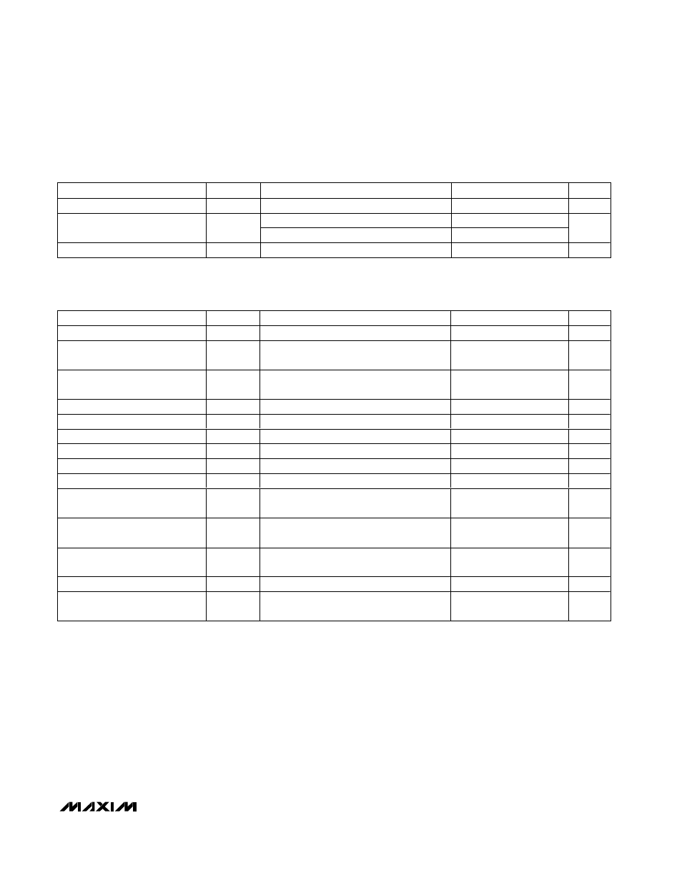
DC ELECTRICAL CHARACTERISTICS (continued)
(V+ = 3V to 5.5V, T
A
= T
MIN
to T
MAX
, unless otherwise noted. Typical values are at V+ = 5V, T
A
= +25°C.) (Note 1)
PARAMETER
SYMBOL
CONDITIONS
MIN
TYP
MAX
UNITS
Pullup to V+ INPUT1, INPUT2
I
PULLUP
26.5
µA
I
SINK
= 6mA, T
A
= -40
°C to +85°C
0.4
IRQ/SEG9, SDA Output Low
Voltage
V
OLBK
I
SINK
= 4mA, T
A
= T
MIN
to T
MAX
0.4
V
SDA Output Low Voltage
V
OL(SDA)
I
SINK
= 6mA
0.4
V
TIMING CHARACTERISTICS
(V+ = 3V to 5.5V, T
A
= T
MIN
to T
MAX
, Figure 1, unless otherwise noted.) (Note 1)
PARAMETER
SYMBOL
CONDITIONS
MIN
TYP
MAX
UNITS
Serial Clock Frequency
f
SCL
400
kHz
Bus Free Time Between a STOP
and a START Condition
t
BUF
1.3
µs
Hold Time (Repeated) START
Condition
t
HD, STA
0.6
µs
Repeated START Setup Time
t
SU, STA
0.6
µs
STOP Condition Setup Time
t
SU, STO
0.6
µs
Data Hold Time
t
HD, DAT
(Note 3)
0.9
µs
Data Setup Time
t
SU, DAT
100
ns
SCL Clock Low Period
t
LOW
1.3
µs
SCL Clock High Period
t
HIGH
0.6
µs
Rise Time of Both SDA and SCL
Signals, Receiving
t
R
(Notes 2, 4)
20 +
0.1C
B
300
ns
Fall Time of Both SDA and SCL
Signals, Receiving
t
F
(Notes 2, 4)
20 +
0.1C
B
300
ns
Fall Time of SDA Transmitting
t
F
(Notes 2, 5)
20 +
0.1C
B
250
ns
Pulse Width of Spike Suppressed
t
SP
(Note 6)
50
ns
Capacitive Load for Each Bus
Line
C
B
400
pF