Rainbow Electronics MAX6959 User Manual
Page 2

MAX6958/MAX6959
2-Wire Interfaced, 3V to 5.5V, 4-Digit,
9-Segment LED Display Drivers with Keyscan
2
_______________________________________________________________________________________
ABSOLUTE MAXIMUM RATINGS
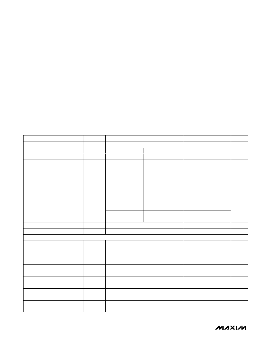
DC ELECTRICAL CHARACTERISTICS
(V+ = 3V to 5.5V, T
A
= T
MIN
to T
MAX
, unless otherwise noted. Typical values are at V+ = 5V, T
A
= +25°C.) (Note 1)
Stresses beyond those listed under “Absolute Maximum Ratings” may cause permanent damage to the device. These are stress ratings only, and functional
operation of the device at these or any other conditions beyond those indicated in the operational sections of the specifications is not implied. Exposure to
absolute maximum rating conditions for extended periods may affect device reliability.
Voltage (with respect to GND)
V+, SCL, SDA .......................................................-0.3V to +6V
All Other Pins............................................-0.3V to (V+ + 0.3V)
Current
DIG0/SEG0–DIG3/SEG3 Sink Current ..........................275mA
DIG0/SEG0–SEG9 Source Current .................................30mA
SCL, SDA, INPUT1, INPUT2 ...........................................20mA
Continuous Power Dissipation (T
A
= +70°C)
16-Pin DIP (derate at 10.5mW/°C above +70°C) .........842mW
16-Pin QSOP (derate at 8.34mW/°C above +70°C).....667mW
Operating Temperature Range
MAX695_ (T
MIN
to T
MAX
) ...............................-40°C to +125°C
Junction Temperature ......................................................+150°C
Storage Temperature Range .............................-65°C to +150°C
Lead Temperature (soldering, 10s) .................................+300°C
PARAMETER
SYMBOL
CONDITIONS
MIN
TYP
MAX
UNITS
Operating Supply Voltage
V+
3
5.5
V
T
A
= +25°C
20
50
Shutdown Supply Current
I
SHDN
Shutdown mode, all
digital inputs at V+
T
A
= T
MIN
to +85°C
125
µA
T
A
= +25°C
5.9
6.7
Operating Supply Current
I+
Intensity set to full,
no display load
connected, INPUT1
and INPUT2 open
circuit
T
A
= T
MIN
to T
MAX
7.5
mA
Display Scan Rate
f
SCAN
4 digits scanned
T
A
= T
MIN
to T
MAX
510
780
1050
Hz
Keyscan Debounce Time
t
DEBOUNCE
T
A
= T
MIN
to T
MAX
30.3
41
63
ms
T
A
= +25°C
-19
-23
-29
V
LED
= 2.4V,
V+ = 4.5V to 5.5V
T
A
= T
MIN
to T
MAX
-18
-30
T
A
= +25°C
-16
-29.5
Segment Drive Source Current
I
SEG
V
LED
= 2V,
V+ = 3V to 5.5V
T
A
= T
MIN
to T
MAX
-15.5
-30.5
mA
Segment Current Slew Rate
∆I
SEG
/
∆t
11
mA/µs
Segment Drive Current Matching
∆I
SEG
4
%
LOGIC INPUTS AND OUTPUTS
Input Leakage Current SCL
and SDA
I
IH
, I
IL
-1
+1
µA
Logic High Input Voltage SCL,
SDA
V
IH
2.1
V
Logic Low Input Voltage SCL,
SDA
V
IL
0.8
V
Input Leakage Current INPUT1,
INPUT2
I
INH
, I
INL
INPUT_ = V+
-1
+1
µA
Logic High Input Voltage INPUT1,
INPUT2
V
INH
0.7
✕
V+
V
Logic Low Input Voltage INPUT1,
INPUT2
V
INL
0.3
✕
V+
V
