Rainbow Electronics MAX7394 User Manual
Page 2
MAX7393/MAX7394
Precision Silicon Oscillators with
Enable or Autoenable
2
_______________________________________________________________________________________
ABSOLUTE MAXIMUM RATINGS
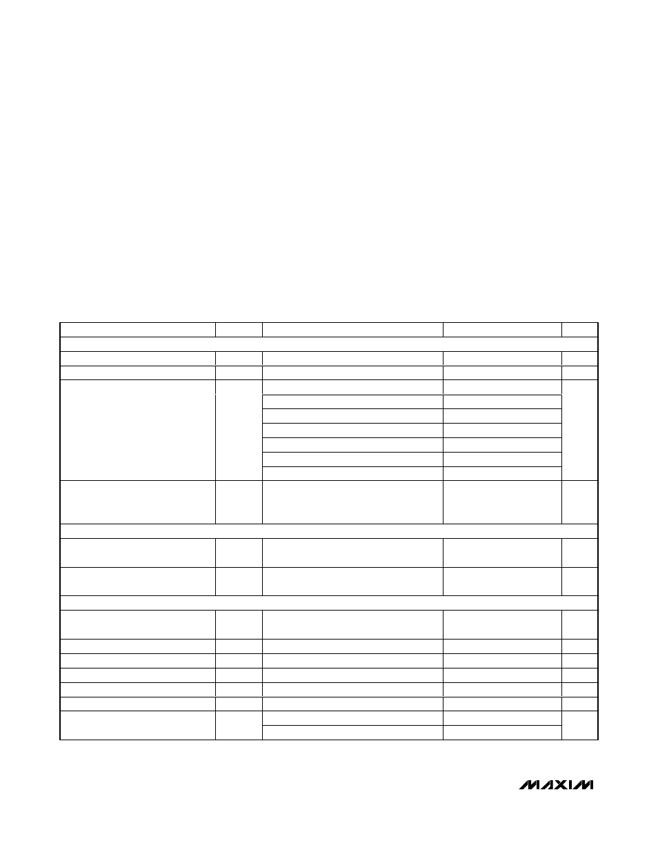
ELECTRICAL CHARACTERISTICS
(V
CC
= V
CC2
= +2.4V to +3.6V, C
L
= 10pF, T
A
= -40°C to +125°C, unless otherwise noted. Typical values are at V
CC
= V
CC2
= +3.3V,
T
A
= +25°C, unless otherwise noted.) (Note 1)
Stresses beyond those listed under “Absolute Maximum Ratings” may cause permanent damage to the device. These are stress ratings only, and functional
operation of the device at these or any other conditions beyond those indicated in the operational sections of the specifications is not implied. Exposure to
absolute maximum rating conditions for extended periods may affect device reliability.
V
CC
, V
CC2
to GND.................................................-0.3V to +4.0V
CLOCK, CLKIN, ENABLE, I.C. to GND ......-0.3V to (V
CC
+ 0.3V)
CLOCK Output Current ....................................................±50mA
Continuous Power Dissipation (T
A
= +70°C)
6-Pin µDFN (derate 4.5mW/°C over +70°C) ................358mW
6-Pin TDFN (derate 18.2mW/°C over +70°C) ............1455mW
Operating Temperature Range .........................-40°C to +125°C
Junction Temperature ......................................................+150°C
Storage Temperature Range .............................-65°C to +150°C
Lead Temperature (soldering, 10s) .................................+300°C
PARAMETER
SYMBOL
CONDITIONS
MIN
TYP
MAX
UNITS
DC CHARACTERISTICS
Operating Supply Voltage
V
CC
2.4
3.6
V
Operating Output Supply Voltage
V
CC2
2.4
3.6
V
922kHz, MAX739_ _ _ _LY
4.4
4MHz, MAX739_ _ _ _RD
5.4
8MHz, MAX739_ _ _ _TP
5.8
16MHz, MAX739_ _ _ _WB
6.5
32MHz, MAX7394_ _ _ YN
9.2
33MHz, MAX7394_ _ _ YQ
9.5
Total Operating Supply Current
(Note 2)
I
TOT
48MHz, MAX7394_ _ _ ZY
12
mA
Total Shutdown Supply Current
I
SHDN
Oscillator disabled,
CLKIN = high (MAX7393),
ENABLE = low (MAX7394) (Note 2)
1
2
µA
LOGIC INPUTS (ENABLE, CLKIN)
Logic Input High Voltage
V
IH
0.7
x V
CC2
V
Logic Input Low Voltage
V
IL
0.3
x V
CC2
V
CLOCK OUTPUT
Output High Voltage
V
OH
V
CC2
≥ 2.4V, I
SOURCE
= 5mA
V
CC2
- 0.3
V
Output Low Voltage
V
OL
V
CC2
≥ 2.4V, I
SINK
= 5mA
0.3
V
Output Rise Time
t
R
(Note 3)
5
ns
Output Fall Time
t
F
(Note 3)
5
ns
Duty Cycle
(Note 3)
47
%
Startup Time
Time for output to stabilize
2
ms
Peak-to-peak jitter, 16MHz (MAX7394)
180
Output Jitter (Note 3)
Peak-to-peak jitter, 48MHz (MAX7394)
140
ps