Ordering information – Rainbow Electronics W49F020 User Manual
Page 18
Preliminary W49F020
- 18 -
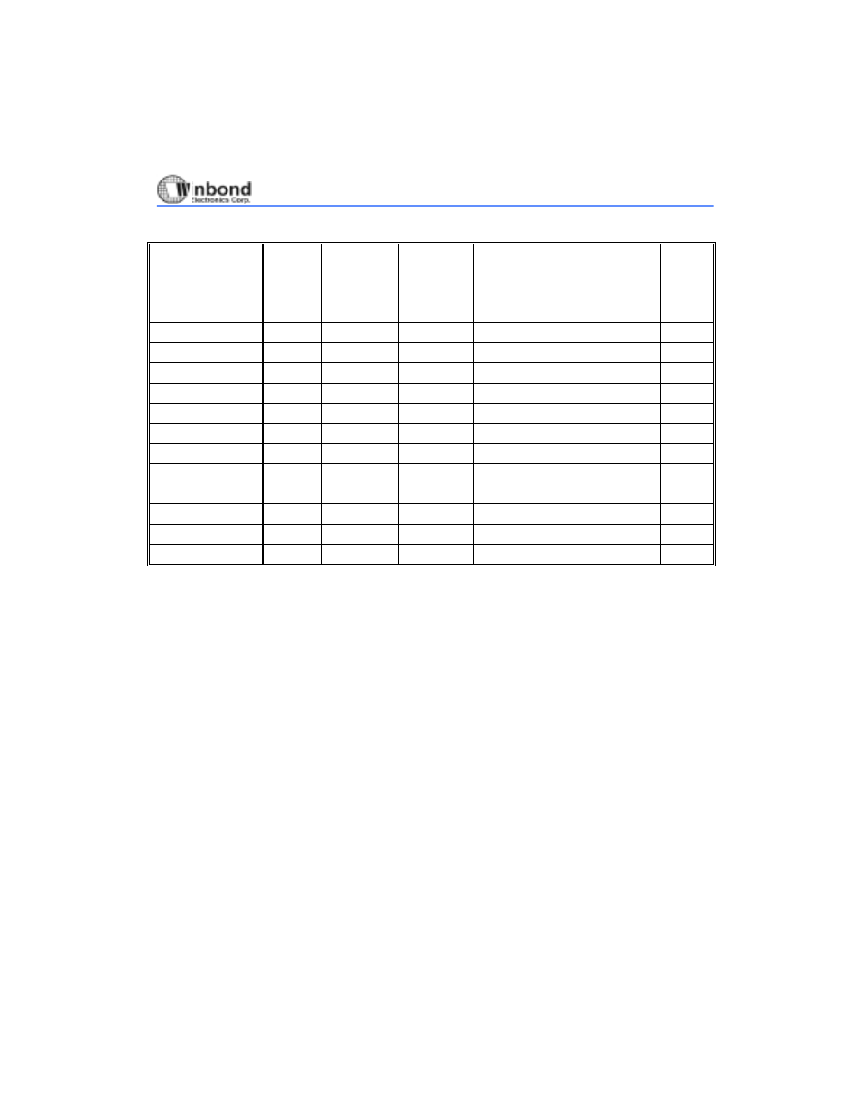
ORDERING INFORMATION
PART NO.
ACCESS
TIME
(nS)
POWER
SUPPLY
CURRENT
MAX.
(mA)
STANDBY
V
DD
CURRENT
MAX.
(
µ
A)
PACKAGE CYCLE
W49F020-70 70
50
100 (CMOS) 32-pin DIP
1K
W49F020-90 90
50
100 (CMOS) 32-pin DIP
1K
W29F020Q-70 70 50
100 (CMOS) 32-pin TSOP (8 mm
×
20 mm)
1K
W29F020Q-90 90 50
100 (CMOS) 32-pin TSOP (8 mm
×
20 mm)
1K
W29F020P-70 70 50
100 (CMOS) 32-pin PLCC
1K
W29F020P-90 90 50
100 (CMOS) 32-pin PLCC
1K
W49F020-70B 70 50
100 (CMOS) 32-pin DIP
10K
W49F020-90B 90 50
100 (CMOS) 32-pin DIP
10K
W29F020Q-70B 70 50
100 (CMOS) 32-pin TSOP (8 mm
×
20 mm)
10K
W29F020Q-90B 90 50
100 (CMOS) 32-pin TSOP (8 mm
×
20 mm)
10K
W29F020P-70B 70 50
100 (CMOS) 32-pin PLCC
10K
W29F020P-90B 90 50
100 (CMOS) 32-pin PLCC
10K
Notes:
1. Winbond reserves the right to make changes to its products without prior notice.
2. Purchasers are responsible for performing appropriate quality assurance testing on products intended for use in applications
where personal injury might occur as a consequence of product failure.
3. There are two kinds of boot block in this device. The part number shown in the Ordering Information table is only for Bottom Boot
Block part, which is in the lower address range. For the requirement of the higher address range boot block, the Top Boot Block,
please contact Winbond FAE for details.