Max5406 audio processor with pushbutton interface, Typical operating characteristics, Electrical characteristics (continued) – Rainbow Electronics MAX5406 User Manual
Page 6
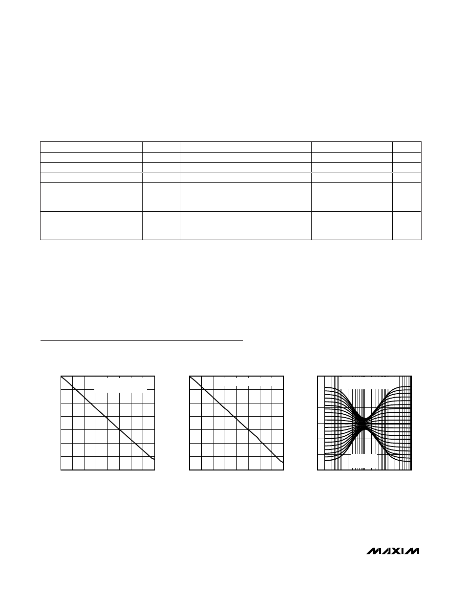
Typical Operating Characteristics
(T
A
= +25°C, unless otherwise noted.)
ATTENUATION vs. TAP POSITION
TAP POSITION
ATTENUATION (dB)
MAX5406 toc01a
0
4
8
12
16
20
24
28
32
-70
-60
-50
-40
-30
-20
-10
0
V
DD
= V
LOGIC
= 5V, V
SS
= 0
VOLUP = 0dB
ATTENUATION vs. TAP POSITION
TAP POSITION
ATTENUATION (dB)
MAX5406 toc01b
0
4
8
12
16
20
24
28
32
-70
-60
-50
-40
-30
-20
-10
0
V
DD
= V
LOGIC
= 2.7V, V
SS
= -2.7V
BAXANDALL CURVE
FREQUENCY (Hz)
GAIN (dB)
MAX5406 toc02a
-15
-10
-5
0
5
10
15
10
100
1000
10,000
100,000
V
DD
= V
LOGIC
= 5V, V
SS
= 0
TREBLE = BASS
C
CB_
= 10nF
C
CT_
= 2.2nF
MAX5406
Audio Processor with Pushbutton Interface
6
_______________________________________________________________________________________
Note 1: All devices 100% production tested at T
A
= +85°C. Limits over the operating temperature range are guaranteed by design.
Note 2: Treble = bass = 0dB. C
CB_
= open, C
CT
_ = short, left input signal = right input signal = +2V.
Note 3: See Tables 3 and 4 and Figure 7. V
DD
= +2.7V, V
SS
= -2.7V.
Note 4: Guaranteed by design.
Note 5: Measured with A-weighted filter.
Note 6: Supply current measured while attenuator position is fixed.
Note 7: Set _OUT = 0dB and shutdown device SHDN = 0. t
WU
is the time required for _OUT to reach 0dB after SHDN goes high.
PARAMETER
SYMBOL
CONDITIONS
MIN
TYP
MAX
UNITS
Power-Up Time
t
PU
Power first applied, _OUT = -20dB
1
s
Wake-Up Time
t
WU
From shutdown (Note 7)
1
s
Logic Supply Voltage
V
LOGIC
DGND = 0, V
LOGIC
≤ V
DD
+2.7
V
DD
V
Logic Active Supply Current
I
LOGIC
No signal, one button pressed, remaining
logic inputs connected to V
LOGIC
or
unconnected
150
µA
Logic Shutdown Supply Current
No signal, all logic inputs connected to
V
LOGIC
or unconnected, SHDN = DGND
(Note 6)
0.2
2
µA
ELECTRICAL CHARACTERISTICS (continued)
(V
DD
= V
LOGIC
= +5.0V, V
SS
= 0, V
BIAS
= V
CMSNS
= V
DD
/ 2, DGND = 0, ambience disabled, V
AMBLI
= V
AMBRI
= V
BIAS,
V
R1_L
=
V
L1_L
= V
R2_L
= V
L2_L
= external V
BIAS
, C
CSUB
= 0.15µF, C
CLS
= C
CRS
= 1µF, C
CBL
= C
CBR
= 3.3nF, C
CTL
= C
CTR
= 4.7nF, C
BIAS
=
0.1µF, C
CBIAS
= 50µF (see the Typical Application Circuit), T
A
= T
MIN
to T
MAX
unless otherwise specified. Typical values are at T
A
=
+25°C). (Note1)