V.35 interface – Rainbow Electronics MAX13175E User Manual
Page 30
MAX13171E/MAX13173E/MAX13175E
Multiprotocol, Pin-Selectable
Data Interface Chipset
30
______________________________________________________________________________________
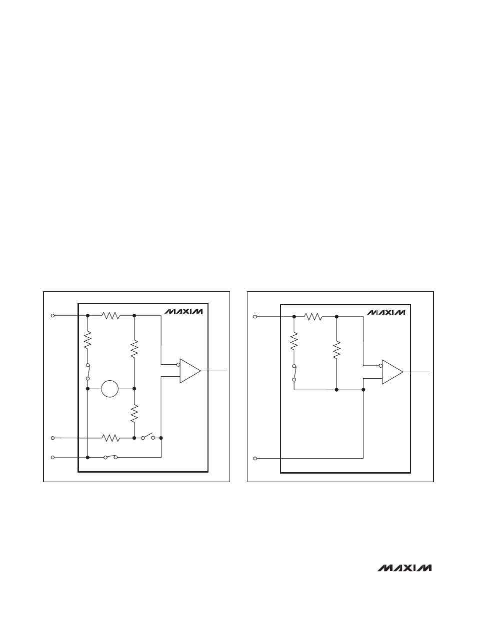
V.28 (RS-232) Interface
The V.28 interface is an unbalanced single-ended inter-
face (Figure 18). The V.28 driver generates a minimum
of ±5V across the 3kΩ load impedance between A’ and
C’. The V.28 receiver has a single-ended input.
The MAX13171E/MAX13173E V.28 mode receivers have
a threshold between +0.8V and +2.0V. To aid in reject-
ing system noise, the MAX13171E/MAX13173E V.28
receivers have a typical hysteresis of 250mV. Switch S3
in Figures 24a and 24b is closed in V.28 mode to enable
the 5kΩ V.28 termination at the receiver inputs.
V.35 Interface
Figure 25 shows a fully-balanced, differential standard
V.35 interface. The generator and the load must both
present a 100Ω ±10Ω differential impedance and a
150Ω ±15Ω common-mode impedance as shown by
the resistive T-networks in Figure 26. The V.35 driver
generates a current output (±11mA, typ) that develops
an output voltage of ±550mV across the generator and
load termination networks. The V.35 receiver is sensi-
tive to ±200mV differential signals at receiver inputs A’
and B’. The V.35 receiver rejects common-mode sig-
nals developed across the cable (referenced from C to
C’) of up to ±4V, allowing for error-free reception in
noisy environments.
In Figure 26, the MAX13175E is used to implement the
resistive T-network that is needed to properly terminate
the V.35 driver and receiver. Internal to the
MAX13175E, S1 and S2 are closed to connect the T-
network resistors to the circuit. The V.28 termination
resistor (internal to the MAX13171E) is disabled by
opening S3 to avoid interference with the T-network
impedance.
The V.35 specification allows for ±4V of ground differ-
ence between the V.35 generator and V.35 load. The
MAX13174E maintains correct termination impedance
over this condition.
R6
11k
Ω
R8
5k
Ω
A
′
B
′
C
′
A
B
GND
R5
55k
Ω
1.4V
R7
11k
Ω
R4
55k
Ω
MAX13171E
MAX13173E
S3
RECEIVER
S2
S1
+
-
Figure 24a. V.28 Termination and Internal Resistance Network
for Receiver 1, 2, and 3
R6
11k
Ω
R8
5k
Ω
A
′
C
′
A
GND
R5
55k
Ω
MAX13173E
S3
RECEIVER
Figure 24b. V.28 Internal Resistance Network for Receiver 4
and 5